RadioRon
Well-Known Member
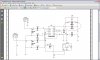
Harros said:Well, I have finished the RF amplifier design, it seems working well (with a gain of approximately 30dB). It seems the tank filter greatly improve the gain of the amplifier... What do you think about this amplifier?
However, there is a problem where the output of the amplifier for the signal with nano volt range is not desirable as the output waveform (the waveform is perfect) is shifted up and down in simulation. It seems its due to input coupling capacitor as I try varying the value of that capacitor and investigate the result waveform for the 1uV-range input, the waveform shifted up and down (similar to the above-mentioned situation) when i adjust the capacitor with the value smaller than it supposed to be... What do you think?
I don't know why the simulation is behaving that way. The input capacitor is normally chosen to have a low impedance compared to the source and load resistances that it is feeding. This implies that the larger the capacitance,the better, but in practice we find that when the capacitance is too big, it begins to have too much series inductance which is undesireable. So, we usually choose something smaller. For example, if we want the capacitor to have an impedance less than 1 ohm then it would have to be 160 nF or larger. Your choice of 100 nF seems ok.
I'm not happy with your choice of base bias resistors. The ratio of base resistors to the emitter resistor is simply too large and cannot be supported by a current gain of only 100 such as the 2n222 might have. You need to either increase the emitter resistor, which will reduce the total collector current, or you have to reduce the base bias resistors so that the base current necessary to drive the emitter resistor doesn't cause a significant voltage drop across the upper base bias resistor.
While the tank circuit topology seems OK, I'm surprised that the tap ratio is so high. You have tapped the 50 ohm load about 90% across the tank circuit, which dramatically reduces the tank's loaded Q. These types of circuits usually work better when the loaded Q is about 10 to 30% less than the unloaded Q.