MrDEB
Well-Known Member
some boards I have done
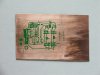
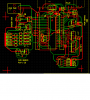
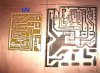
This is using the PULSAR method with printer density set at 5
These came out nice.
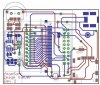
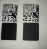
Working on a daughter board w/ LCD to make a simple daughter board to try out the different density setting and hopefully no smudges.
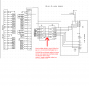
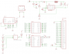
need to find a better method to show a ribbon cable connection between two jacks
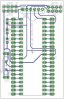
This is using the PULSAR method with printer density set at 5
These came out nice.
Working on a daughter board w/ LCD to make a simple daughter board to try out the different density setting and hopefully no smudges.
need to find a better method to show a ribbon cable connection between two jacks