Torben said:
And your results have made me consider setting up a UV etching kit.
Awesome! That was the goal -- to show people just how easy it can be, and the results you can achieve.
As I said, I have never tried the toner method -- I have been reading up on both methods for a week or so before deciding. Even then it was "just make a decision, man!". It really was the paper scrubbing and touch up of the toner method that made me try the UV method though. The toner method is appealing though, simply because of how easy (and inexpensive) to get setup -- yet, I am happy with the method I choose -- works for me!
")
Let's see, I spent the following to get setup;
1 x 750ml Developer $10.50
1 x 750ml Ferric-Chloride $7.00
2 x 6" x 8" pieces of glass (off cuts) $1.99
1 x package of transparency $7.95
1 x Presensitized Copper Clad Board $7.95
1 x Plant Grow bulb (dollar store) $0.99
1 x light fixture (hood) $6.00
Everything else I had (foam brush, gloves, glasses, plastic containers (the throw away tupperware stuff), tape, etc.), but even if you had to buy this stuff, we're still talking only another $10, tops.
So, even with the extra stuff I had, it works out to $52.38 (yeah, plus tax!). At Sayal Electronics, I saw they had a devloping kit for $45, the UV light for $40 and the etching kit for $40 -- $125 gets you setup with everything I listed (plus two extra PS Copper Boards) and a nice tank with bubbler for etching (I use a throw away tupperware and slosh!). Either way, you can do quite a few boards with what you have (especially if you prepare and do a bunch at a time so you're not wasting alot of chemicals to do one board).
So, I hope you give it a try -- YOU CAN DO IT! (Every time I say that, I picture Rob Schneider with a beer in hand in "The Waterboy"!
")
)
PS - that magnifying hood really freaks me out!


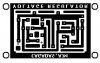
 What did you use for layout software?