Electro Tech is an online community (with over 170,000 members) who enjoy talking about and building electronic circuits, projects and gadgets. To participate you need to register. Registration is free. Click here to register now.
Welcome to our site! Electro Tech is an online community (with over 170,000 members) who enjoy talking about and building electronic circuits, projects and gadgets. To participate you need to register. Registration is free. Click here to register now.
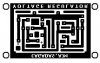
Oh, right, one of the "important notes" I was trying to remember to mention slipped past me (someone would have noticed though)!
The "pads" of the ICs are, well, not really pads at all by default -- just small circles -- not good when you need to drill though them. Well, I would think that the proper way to do it would be to drop in your ICs, then go back and add whatever style of pads to them. Anything that had square pads worked out great.
Oh, and if you're wanting any kind of writing on the board (such as I did), you have to do it BACKWARDS! Remember, when you are doing a single sided board and doing bottom copper, you are looking THROUGH the board from the component side. Obviously, I only understand that now!
Wow, thats an awsome lookin PCB What did you use for layout software?
I really want to try this myself, but I can't get the hang of Eagle at all. I downloaded the demo for Sprint Layout, and that looks easier to learn, but you can't print anything with the demo, and I have not yet found a place to buy it that is in the US or just has a price in US dollars
The "pads" of the ICs are, well, not really pads at all by default -- just small circles -- not good when you need to drill though them. Well, I would think that the proper way to do it would be to drop in your ICs, then go back and add whatever style of pads to them. Anything that had square pads worked out great.
The way I did it was define a smaller drill size in Eagle and edited the IC pads to be larger. I guess those tiny pads are fine if you are getting a professional PCB made and every hole is plated through, but it's a bugger if you are drilling by hand.
Do not give up on Eagle. It is worth the extra effort it takes to learn. You can ask questions here or in Eagles own support group. In Eagle you set the drill size. The pad size is determined by restring. Restring sets the copper pads size as a percentage of the drilled hole. Larger percentages makes larger pads for a given size hole. For boards that are to be drilled by hand there is a script called DRILL-AID. It reduces the size of the hole on the artwork. The smaller hole can be used to center the drill on the etched board.
I usually do my PCB layout using paint. What I do is that I print the layout in a transparency and Iron it on the PCB until the entire layout sticks on the PCB. Can I ask any suggestions on what to do?
Do not give up on Eagle. It is worth the extra effort it takes to learn. You can ask questions here or in Eagles own support group. In Eagle you set the drill size. The pad size is determined by restring. Restring sets the copper pads size as a percentage of the drilled hole. Larger percentages makes larger pads for a given size hole. For boards that are to be drilled by hand there is a script called DRILL-AID. It reduces the size of the hole on the artwork. The smaller hole can be used to center the drill on the etched board.
Do not give up on Eagle. It is worth the extra effort it takes to learn. You can ask questions here or in Eagles own support group. In Eagle you set the drill size. The pad size is determined by restring. Restring sets the copper pads size as a percentage of the drilled hole. Larger percentages makes larger pads for a given size hole. For boards that are to be drilled by hand there is a script called DRILL-AID. It reduces the size of the hole on the artwork. The smaller hole can be used to center the drill on the etched board.
Ditto--Eagle was a bit of a pain to get used to, but it gets easier and is worth it for what you end up being able to make it do. And lots of help is available if you get stuck! And drill-aid rocks, especially if you are using a hand drill or if your drill press has some runout.
To Kyle: very nice first board. You even nailed the lettering. Good job.
The schematics and layout software was Proteus, ISIS and ARES respectively. I don't know about Eagle as I have never used it. I'd say stick with whatever you've got and learn it -- even if it's MSPaint (as mentioned above). It's really what you learn more that the software -- you can learn to draw the layout in any format -- it's just nice to have some of the "fancier" programs to make the process a little more enjoyable, and quicker. Even Proteus was a challenge to learn.
I'll have to take a look at DRILL-AID -- what I did was use a pad (any pad that I actually laid on the board, not from an IC) with a small inside hole size. It did assist greatly in centering the bit. All-in-all, I am not disappointed in how the holes turned out -- it was all a learning experience. They only get better from here!
@paparts --> I've never done a PCB before, so last week I started reading up on the subject (mostly in these forums). I just didn't like the idea of ironing on the artwork. Every article that I read on transferring, it just seemed like the lines didn't come out well enough (well enough for my liking anyway) and you had to "touch them up" with an etch resistant marker -- that just made for ugly lines, IMHO. I'm not trying to run that method down, just trying to explain why I went with the "photosensitive" method.
I've never used Proteus before, but from what I understand, the software you're using should probably take care of anything Eagle does and possibly more.
And your results have made me consider setting up a UV etching kit. I've used toner transfer up until now, with varying results. When it works well for me, it works quite well, but sometimes it takes a few runs to get the ironing just right. And yeah, the time spent rubbing excess paper off the board before etching and fixing up traces with a Sharpie is a bit of a pain.
Awesome! That was the goal -- to show people just how easy it can be, and the results you can achieve.
As I said, I have never tried the toner method -- I have been reading up on both methods for a week or so before deciding. Even then it was "just make a decision, man!". It really was the paper scrubbing and touch up of the toner method that made me try the UV method though. The toner method is appealing though, simply because of how easy (and inexpensive) to get setup -- yet, I am happy with the method I choose -- works for me!
Let's see, I spent the following to get setup;
1 x 750ml Developer $10.50
1 x 750ml Ferric-Chloride $7.00
2 x 6" x 8" pieces of glass (off cuts) $1.99
1 x package of transparency $7.95
1 x Presensitized Copper Clad Board $7.95
1 x Plant Grow bulb (dollar store) $0.99
1 x light fixture (hood) $6.00
Everything else I had (foam brush, gloves, glasses, plastic containers (the throw away tupperware stuff), tape, etc.), but even if you had to buy this stuff, we're still talking only another $10, tops.
So, even with the extra stuff I had, it works out to $52.38 (yeah, plus tax!). At Sayal Electronics, I saw they had a devloping kit for $45, the UV light for $40 and the etching kit for $40 -- $125 gets you setup with everything I listed (plus two extra PS Copper Boards) and a nice tank with bubbler for etching (I use a throw away tupperware and slosh!). Either way, you can do quite a few boards with what you have (especially if you prepare and do a bunch at a time so you're not wasting alot of chemicals to do one board).
So, I hope you give it a try -- YOU CAN DO IT! (Every time I say that, I picture Rob Schneider with a beer in hand in "The Waterboy"! )
I have done both UV exposure and toner transfer. Good and bad results can be had with UV exposure and toner transfer. To get good results with UV it is best to use presensitized boards. You have to get exposure and developing steps right. Wrong times or tired weak chemicals can screw things up. With toner transfer you get good results with Pulsar or P&P transfer paper in conjunction with a laminator. If you use other paper it can be hit and miss, as it using a clothes iron. With either method it is a matter of using the right materials and procedures. Both work. It may be possible to get finer lines with UV exposure. I can get two lines between IC pads with toner transfer. Do not need better then that. No touchup needed. Having said all that....Your board looks good, congratulations.
The nice thing about doing you own PCBs by whatever method is that you can stop hand wiring prototypes. The more you do the better/faster you get. Regardless of how you make the board you should visit the pulsarProFx site and checkout what he is doing for a silscreen. --- I do it a bit different. After the board is etched I paint the top side of the board white with fusion paint. Use toner transfer to place the black silkscreen layer over the paint. I seal it with clear conformal coating to keep it from scratching off. The only problem is that after you paint the board you can not use anything other then soap and water to clean it. Most anything else will mess up the paint and artwork. The liquid fluxes I have also mess up the board. --- One problem with DIY boards is that they do not solder as easy as ones made in a board house. After the board is etched I clean the copper and spray it with a thin coat of conformal coating. The coating keeps the copper from oxidizing. The conformal coating does not seem to bother the soldering process. Maybe the iron vaporizes it. Not sure but they do solder well.
Excellent information there, 3v0 -- thanks for the link. Quite impressive (and why I didn't knock the toner transfer method -- only stated why I chose the method I did! ).
I am still amazed at the quality you can produce yourself. I guess it's been a long time since I looked at home-made PCBs!
I've been making them constantly for the past few days. My supplier of LEDs asked me a couple of months ago if I could make them up some demo PCBs to showcase their products on and I accepted the challenge.
Problem is that every component has a different footprint, different pin sizes and there are some obscure pin spacings.
On top of that, the writing for the component part numbers is etched on the top surface of the board so double sided boards are necessary.
I've got nearly 3000 holes to drill by hand over the next 2 days in a variety of 8 different hole sizes.
Apart from that making your own home PCBs is great fun
Im printing the layout about 4 copies and iron them all or less before I get the perfect layout. How do you toner method and UV? do I need kits or something?
If you had a few months, you could have sent the boards off to have them made.
If you used Eagle and PCB-Gcode you could have a CNC drill the holes. You could have provided the Eagle parts library to your supplier and he could have made them available to his customers.
This site uses cookies to help personalise content, tailor your experience and to keep you logged in if you register.
By continuing to use this site, you are consenting to our use of cookies.

")