Continue to Site

Welcome to our site!

Electro Tech is an online community (with over 170,000 members) who enjoy talking about and building electronic circuits, projects and gadgets. To participate you need to register. Registration is free. Click here to register now.

  • Welcome to our site! Electro Tech is an online community (with over 170,000 members) who enjoy talking about and building electronic circuits, projects and gadgets. To participate you need to register. Registration is free. Click here to register now.

MOSFET operation

Status
Not open for further replies.
TheOne said:
Enlighten me, where do you get the 3Vds from? I don't have my glasses on but I think that I see a value of about 1.25V-1.50 @ 10A :?:

yeah looks more like a little under 2v now that i actually look at it. still, about 20 watts is a lot of power when it can be reduced to less than half that by just switching mosfets.
 
fabbie said:
Hi hi,
IM rather confuse with MOSFET operations on how it works. If i intend to saturate a N-channel MOSFET, all i have to do is overcome its threshold voltage is it? IS the MOSFET Vgs similar to the BJT's Vbe?

Be aware that the term "saturation" only means turning a transistor into a low resistance "ON" state, like a switch, only when referring to BJTs.

Due to the total anarchy in the electrical engineering world, much like how we never decided once and for all which way current "flows", "saturation" means the EXACT opposite for MOSFETs. It means the magnitude of current through the drain-source is being controlled by gate voltage. If the gate voltage is high enough that it leaves the MOSFET in a low impedance state from drain-source for that circuit, it is now OUT of the saturation region.

Stupid engineers.
 
THX THX.
Supposing my Vgs is 5V. Looking at the Vgs Versus Id curve, my Id would be around 15A. Is this how i plot my load line for my Y-AXIS? using the 0V(Vds) and 15A(Id). For motors, the resistance depends on the load, therefore i dont think i can use the I=V/r
 

Attachments

  • curr_109.jpg
    curr_109.jpg
    53 KB · Views: 456
I forgot to ask one more thing. Since the load line would determine the power dissipation and Vds, then What is the Rds(on) for? I thought that as long as the MOSFET was ON, we would able to use the Rds(on) which is equal to 0.077ohm. Assuming we have a current,Id of 5A, the Vds=RdsxId=0.077x5=0.385V. However, looking from the load line, the Vds is apporximately 2V.Is there a relation between the load line and the equation i just calculated here?
 
Rds(on) is measured at specific values of Id and Vgs. For instance, on the IRF540N, Rds(on) is measured at Id=16A and Vgs=10v.

Rds(on) gives a good linear approximation of the equivalent resistance of the MOSFET when it is in the OHMIC region (not saturation)

so as long as you are switching it with a high enough gate voltage to keep it from going into saturation at high current, then Rds(on) is a good approximation of the equivalent resistance of it as a switch.
 
ok i understand. thank you very much. But i still dont get the LOAD LINE part.
When i use the formula Vds=Rds x Id, i will be able to obtain the voltage drop across the Drain-Source. By obtaining the Vds, i would be able to calculate the power dissipation of the mosfet.
However, it seems that each of you(experts) calculate using power dissipation using the load line. Is there any difference or am i getting this all wrong?
 
The power dissipation is always going to be Vds*Id. the load line is used to find the actual values of Vds and Id when using it with a specific power supply voltage and load resistance. (the operating point) from there you can of course calculate power dissipation.
 
evandude said:
P=Vds*Id. at 3 volts and 10 amps, that's 30 watts of power dissipation. using a better MOSFET you can easily get a value of Vds more like less than one volt for a drain current of 10 amps, which will cut your power dissipation immensely. The more power you are dissipating in the transistor, the less power is going to your motor.

I've understand what you have explained previously. But finding the Vds using (Vds=Rds x Id) is really bothering me. The Vds calculated here provide such a small value. However, using the load line, the Vds IS awfully BIG. This part is killing me.

Thx for any explanation
 
why don't you show us some calculations.

bear in mind, that Rds depends on Vgs. the higher Vgs is, the lower Rds becomes. Rds is often measured around 10v for Vgs, whereas if you are operating it at Vgs=5v then Rds is going to be higher than the rated value.
 
If you have a spare pin on your PIC that you can output a square wave from you can easy generate your own 9v auxiliary supply to drive the gates from, as in the attached picture. If you use shottkey diodes like a BAT43 for example you can come very close to almost doubling your voltage.

From this 9v supply you can now power gate drivers (NPN-PNP pair) and still switch these drivers from the PIC. This will now allow you to get the gate on-voltage above 5v to reduce the Rds-on. You can also use a dedicated mosfet driver https://www.electro-tech-online.com/custompdfs/2004/12/fn7113.pdf

The yellow lines represent the GND reference for each channel on the scope. As you can see the base of the wave on chan B is elevated by about 4.5v above GND

All made possible by the principle of DC-restoration :)
 

Attachments

  • 9v_supply.gif
    9v_supply.gif
    26.2 KB · Views: 431
  • driver_150.gif
    driver_150.gif
    6.7 KB · Views: 428
Since i will be using this H-bridge my power supply would be 12V. This would also mean that my Vds is 12V. Looking at the connection, my Vgs is also 12V(correct me if im wrong, MY H-BRIDGE diagram is located below).

The mosfet i bought is the BUZ71A. Plotting the load line, my MAXIMUM current my motor can draw would be around 7A. Therefore i set my Y-AXIS Id as 7A. Since my power supply is 12V, i set my X-AXIS,Vds at 8V(the X-AXIS ends at 8V Vds, there is no 12V. hope im right). Looking at the load line, my Vds is less than 1V and current around 6A.
P=VI=6W. This seem abit weird. Although the calculation shows that the mosfet is efficient, the power dissipation seems awfully low .

OK, here is the part that im confused with. Vds= Rds(on) x Id.
With my Vgs at 12V, i should be able to get a good Rds reading. Looking at the Rds Vs. Id curve, i should be able to get 0.1ohm as my Rds.
Therefore, with actual current i obtain from the load line which is 6A, Vds= Rds x Id = 0.1 x6 = 0.6V.
So, WHY ARE THERE 2 METHODS TO FIND Vds??? 1 from actual load and 1 from Vds=Rdsx Id. Are they actually the same thing?!

By the way, pls tell me whether my load line analysis and calculation is correct. I MUST GET THIS RIGHT!!! Thank you very much!!!!!
 

Attachments

  • mosfetmod.jpg
    mosfetmod.jpg
    47 KB · Views: 383
  • loadline.jpg
    loadline.jpg
    40 KB · Views: 427
  • rds.jpg
    rds.jpg
    41.7 KB · Views: 393
Look at the 2 diagrams, the input Hi and Lo levels are generated by the switches in the diagram (I had to increase the cap values as I can't change over the switches that fast in the simulation to prevent some discharge of the caps) The PIC will of course do that at 10KHz

OK, assume the input side of C1 is low (STEP1). C1 will now charge to (5v-1d) and C2 to (5v-2d) where d is the voltage drop over the diode. Now when the input of C1 is forced up to the +5v on the rising edge of the input (STEP 2), this now effectively places the -ve side of C1 on top of the 5v supply. Because the +ve side is now above the 5v line, D1 will now be reverse biased and a voltage of (C1v + 5v) will now be transferred to C2 through D2. The voltage will make the level on C2 to rise up to about 2 times the supply voltage. In this process C1 will discharge, ready for the cycle to repeat again.

It is of course important that the input signal can supply enough current to charge-discharge the input cap quickly and that C1 and C2 are large enough to prevent too much drop in the output voltage as the charge on C2 leaks away into the load connected to it.
 

Attachments

  • 9v_operation.gif
    9v_operation.gif
    10.2 KB · Views: 370
fabbie said:
By the way, pls tell me whether my load line analysis and calculation is correct. I MUST GET THIS RIGHT!!! Thank you very much!!!!!

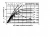
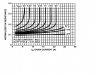
You are reading figures on your graph for pulsed operation (80uS) and 50% duty cycle. You will be much better informed by looking at the curves for DC operation (assuming that is what you want to do) to see what you need to stay within the safe operating area (SOA). Also remember that a lot of times these curves are plotted for a mounting base of 25 deg C, which is very difficult to maintain in practical applications. The SOA would be less for higher mounting base temp's.

Ptot(DC) = [T(junction-max) - T(mounting base)]/[Rthermal(junction -> mounting base)]

Where Ptot is the power dissipation you may have at DC operation in the device, taking into account the other parameters in the formula.

Rthermal(j-mb) you will get under the thermal data and is usually in Kelvin/Watt, which states how much the junction temp of the device will increase for every watt dissipated in the device. Typical T(junction-max) will be 175 deg C. So it is clear from the formula that the cooler you keep your devices on a heatsink, the more power you can handle without melting the junction material.

The graph of normalized on-resistance vs temp is used to see the multiplication factor to use with Rds-on at higher temp's. Remember I said measurements are taken at 25 deg C. If you look at the graph, you will notice that the multiplication factor at 25 deg C is 1.0 :eek: . Since it is almost impossible to operate the device while keeping the junction at 25 deg C, you should be aware that Rds-on will be higher by the multiplication factor from the graph, depending on what the junction temperature will be.

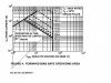
At a heatsink temp of 60 deg C, your device will only be able to dissipate about 30W

:!: Another thing, Rds-on quoted in the quick reference data often refer to pulsed operation with a junction temp at 25 deg C. Always make sure at what temp the data is quoted as these figures can be misleading and rarely obtainable in real applications.

It is very dangerous to read only parts of datasheets (graphs), without taking all the factors into account!
 
Do you mind explaining how the SOA curve works?? It does not even show the Vgs and saturation line.
And it seems that all the other curves in this datasheet are drawn with the pulse duration of 80us and duty cycle 0.5 . There are no DC lines. What should i do?
LAstly, when people plan to buy and use the MOSFETs, do they look at EACH graph one by one ?? sounds really tedious (not that im complaining).
Forgot to add, does the MOSFET gate require current? It seems that no one ever mentions about the gate current. For BJTs, base current is really important.
 

Attachments

  • soa.jpg
    soa.jpg
    45.6 KB · Views: 298
Status
Not open for further replies.

Latest threads

New Articles From Microcontroller Tips

Back
Top