Continue to Site

Welcome to our site!

Electro Tech is an online community (with over 170,000 members) who enjoy talking about and building electronic circuits, projects and gadgets. To participate you need to register. Registration is free. Click here to register now.

  • Welcome to our site! Electro Tech is an online community (with over 170,000 members) who enjoy talking about and building electronic circuits, projects and gadgets. To participate you need to register. Registration is free. Click here to register now.

mosfet load switch

Status
Not open for further replies.
What is the voltage you want it to disconnect at (Vu)?
What is the voltage you want it to reconnect(Vl)?

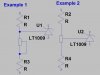
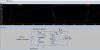
If you are separately switching the load on/off, you need a minimum load resistance (~100K) between the drain of the pFet and ground to pull the right end of the 2.2meg resistor to ground if the load is missing.

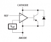
Obviously, Vu and Vl must be above the Vref (2.495V) of the TL431. I am using the 431 as a comparator where the Ref input is compared to the internal Vref of 2.495V and when Ref>Vref the Cathode is pulled down to ~2V. The minimum Vl and Vu is then determined by the sum of Vt of the PFet (~4V?) plus the 2V drop from cathode to anode, which means that the circuit will work when Vcc is >~6V

To compute Vu and Vl algebraically, follow this:

Call the resistance from cc to ref R1, so R1=26200+500=27200
Call the resistance from ref to gnd R2, so R2=10000+500=10500
Call the feedback resistor R3, R3=2200000

When the input V(cc) is initially low, the load pulls V(out) to 0V, effectively putting R3 in parallel with R2.

R' = R3*R2/(R3+R2) = 2200000*10500/(2200000+10500) = 10450

Now use the voltage divider equation to compute the switching point V1:

2.495 = V1*R'/(R1+R')

solving for V1, V1=2.495*(R1+R')/R' = 2.495*(27200+10450)/10450 = 8.989

Similarly, when Vcc is initially high, and decreasing, the other switching point occurs with R3 in parallel with R1, so R'' = R1*R3/(R1+R3) = (27200+2200000)/(27200+2200000) = 26868

2.495 = V2*R1/R1+R'')

V2 = 2.495*(R1+R'')/R1 = 2.495*(10500+26868)/10500 = 8.879

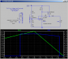
So, the hysteresis is V1-V2 = 0.110

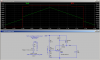
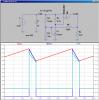
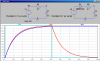
Here is a sim showing the hysteresis in this example.
 

Attachments

  • Hyst.png
    Hyst.png
    31.7 KB · Views: 280
I am trying to switch the load on at 10V, switch the load off at 9V.
 
I am trying to switch the load on at 10V, switch the load off at 9V.

What is the load resistance?

What PFet are you using?
 
why not use a comparator it is much easier

He'll have the same set of questions about how to achieve the desired hysteresis with a comparator. After all, what is a LM431, it is a comparator with one input already tied to a 2.495V reference!
 
basically you are asking for a circuit very similar to the NE555 timer internals but with different thresholds, I suggest you use it as a basis of your design
 
the mosfet is a Si3443CDV. The load is the equivalent to 8R (12v / 1.5A). Although its not actually a resistive load, the pc i am powering runs from 12V down to 9V. So its prob more a constant power load.

Ive attached the circuit i have.

Power supply is 12V, Ignore LT1009 text.
 

Attachments

  • circuit.jpg
    circuit.jpg
    42.2 KB · Views: 733
Last edited:
I changed resistor values and the pot wiper position to achieve your trip points. I also changed the PFet model. I posted this before I saw your proposed circuit. Note I am using higher value resistors to set the trip points.
 

Attachments

  • Hyst1.png
    Hyst1.png
    30.2 KB · Views: 242
Last edited:
Hi Mike

That is excellent, just what ive been trying to do in LTspice but finding it a slow learning curve. Should the load current not be proportionate to Vin after switch on. The graph looks a little flat.

Thanks again.
 
... Should the load current not be proportionate to Vin after switch on. The graph looks a little flat.

It is. I vary the input (Vcc) over a narrow range.
 
I changed resistor values and the pot wiper position to achieve your trip points. I also changed the PFet model. I posted this before I saw your proposed circuit. Note I am using higher value resistors to set the trip points.

Why are there 4 resistors in the potential divider part of the circuit. Is this how LTspice interprets potentiometers? R4 and R3 are actually the pot, and in the above example is set to 560R?

Is it best to use the wiper of the pot connected directly to the ref pin or can you tie the wiper pin to one of the other pins (top / bottom of pot) and use it like a variable resistor.
 
Yes, the two resistors model the behavior of the pot as the wiper is moved. Note that if the parameter K changes, that causes one resistor to get bigger while the other automatically gets smaller.

By connecting the two fixed resistors at the ends of the pot, it desensitizes the pot so moving the wiper is not so touchy. This is the electrical version of a a hundred-turn pot :D

Look at the internal schematic on the data sheet for the LM431 below. Note that the Ref pin connects to an non-inverting input of an opamp. Connecting the wiper to there tricks the LM431 to acting as a comparator; with the output being taken at the anode pin. Since the opamp is running open-loop, and it has a gain of ~40K, it does a pretty good job of acting as a comparator.

The positive feedback that comes through the high value resistor from the output to the Ref pin is what gives the circuit positive feedback (snap action) and the required hysteresis.
 

Attachments

  • intern.png
    intern.png
    6.5 KB · Views: 262
Last edited:
Yes, the two resistors model the behavior of the pot as the wiper is moved. Note that if the parameter K changes, that causes one resistor to get bigger while the other automatically gets smaller.

By connecting the two fixed resistors at the ends of the pot, it desensitizes the pot so moving the wiper is not so touchy. This is the electrical version of a a hundred-turn pot :D

Look at the internal schematic on the data sheet for the LM431 below. Note that the Ref pin connects to an non-inverting input of an opamp. Connecting the wiper to there tricks the LM431 to acting as a comparator; with the output being taken at the anode pin. Since the opamp is running open-loop, and it has a gain of ~40K, it does a pretty good job of acting as a comparator.

The positive feedback that comes through the high value resistor from the output to the Ref pin is what gives the circuit positive feedback (snap action) and the required hysteresis.


what is the prefered way, i think both work and have the same effect but perhaps i am not seeing something.
 

Attachments

  • pot.jpg
    pot.jpg
    32 KB · Views: 353
The second one has the advantage that it is easier to analyze. The current flowing down through the pot does not change as the pot wiper is moved.
 
After all, what is a LM431, it is a comparator with one input already tied to a 2.495V reference!

It is not a comparator... it's a op-amp.

If 2.49V is to high a TLV431 is a 1.24V reference... just keep in mind that these things like 1mA of cathode current to work properly.
 
I am having trouble simulating this circuit in LTspice. I want to charge the capacitor with a 12V input pulse. Pulse duration should be long enough to charge to 95% level. Then i want to drop the input voltage and power the circuit purely from the capacitor. i can model the capacitor charging ok but using a charged capacitor to power another circuit does not work for me.

Any ideas?

https://www.electro-tech-online.com/attachments/circuit-jpg.41837/
 
Last edited:
Can you post your .asc ?
 
There are several problems with your conceptual schematic and the way you are simulating it.

1. If V1 is a fixed voltage source, there must be a switch between the source and the super cap, otherwise all of the current drawn by the load will ALWAYS come from the source. If you model the source as a time-varying voltage, you will have to add a diode between the source and the supercap to prevent the supercap from discharging backwards into the source. Remember that voltage sources in LTSpice are ideal (unless you specify a series resistance), and current will flow through them in both directions, depending on an external higher voltage. Cutting the wire between the top of the 4.7Ω and the cathode of the Schottky diode would sort of do this, except that the super cap can still discharge backwards into the source if the source voltage dips below the instantaneous supercap voltage.

2. There must be a resistor connected from PFet source to PFet gate to pull the gate high (PFet off) when the TL431 turns off. That new resistor must be able to source at least 1mA when the TL431 is turned on. Look at the circuit I posted earlier. It had that resistor.

Here is a hack at it. Note the use of a current source. It can only supply 0.25A, while the load draws about ~1.5A, meaning that the circuit has to wait for the capacitor to charge, and then disconnect the load when the capacitor voltage discharges to the lower limit. Again, I raised the impedance of the three resistors around the Ref input to the TL431. I iterated on the values until the trip points are 12 and 9V, respectively.

I'm appending the .asc file so you can play with it some more.
 

Attachments

  • LoadDisconnect1.png
    LoadDisconnect1.png
    38.8 KB · Views: 313
  • LoadDisconnect1.asc
    1.6 KB · Views: 172
Last edited:
Hi Mike,

ive attached the .asc file. ive tried various loads and the capacitor still seems to discharge at the same rate, almost at the same rate at which Vin drops. Perhaps this is the Vsource (without internal resistance) you speak of.

Note:

switch.zip is older schematic than one shown in screen shot. adding series resistance does not make much difference.

oh forgot to add tags,

Green - Vin
Blue - Vout
Red - Vcap
 

Attachments

  • switch.zip
    740 bytes · Views: 153
  • Switch3.jpg
    Switch3.jpg
    74.2 KB · Views: 271
Last edited:
You need to understand what is going on in this simplified circuit. Compare the behaviour of these two circuits V(X) and V(Y).
 

Attachments

  • Dd1.png
    Dd1.png
    27.4 KB · Views: 265
Status
Not open for further replies.

Latest threads

Back
Top