Continue to Site

Welcome to our site!

Electro Tech is an online community (with over 170,000 members) who enjoy talking about and building electronic circuits, projects and gadgets. To participate you need to register. Registration is free. Click here to register now.

  • Welcome to our site! Electro Tech is an online community (with over 170,000 members) who enjoy talking about and building electronic circuits, projects and gadgets. To participate you need to register. Registration is free. Click here to register now.

mosfet gate terminal spikes !

Status
Not open for further replies.

qwertyqwq

Member
salut a tt!
i have a problem about full bridge mosfet configuration. The problem is spikes. There are lots of unwanted spikes at the mosfet's gate terminals.
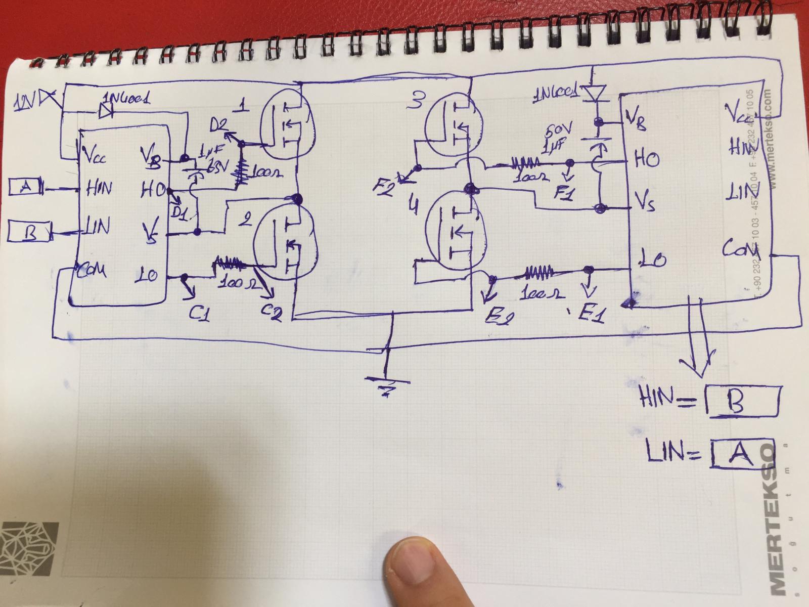
WhatsApp Image 2019-08-01 at 10.38.47.jpeg


This is the scheme of my circuit. Its pretty simple. There are two different signals A and B, which is created by another circuit. The freq of the A and B are 25kHz. There are two mosfet drivers (IR2101) and four mosfets(irfz44n). There are some changes at scheme. Im using FR207 againts 1n4001 , 10uF 63V capacitors against 1uF bootstraps and seperated 12V power supplies. That is all.
The signal A and B are pretty well working. There is no problem about he signal A and B. And also all elements of the circuit has been changed several times but result is not changin.

The problem is #SPIKES. After the mosfet driver's HO pins, there are spikes although main signal are turn off.
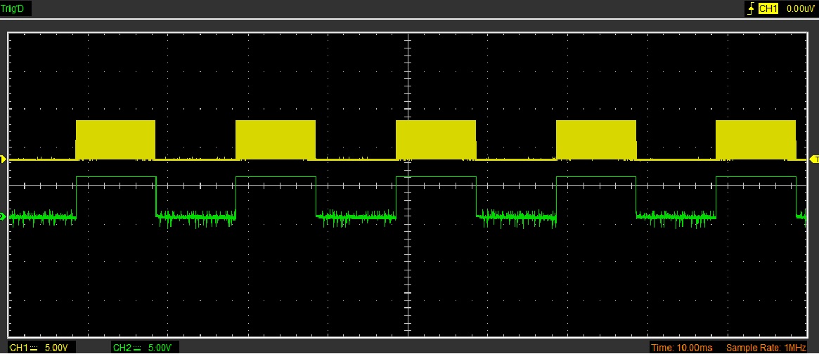
2.sürücü b-f1.jpg


Ch1 is signal B which is before the mosfet driver and i want to see. Dont care to Ch2 (it was old problem).
Signal A is exectly same of the signal B but there is a phase shift about 180 degrees. When the first group of mosfets are switched turn on , the other group of the mosfets will turn off. It must be normal working of full h-bridge.
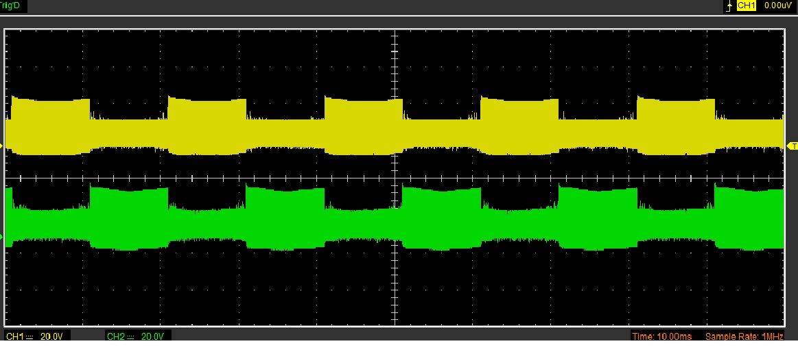
sonhali.jpg

But this is what im seeing. The Ch1 is HO pin of the very left mosfet driver's and Ch2 is HO pin of the very right mosfet driver's. There are lots of spikes when the mosfet should turn off. The spikes are exectly matching the other channels PWM switching signals. Also i should say that ,the problem is only containing HO pins of the both mosfet drivers. The LO pins are working fine and there is no problem about the signal at all. When i remove the drain cable of the top mosfets ( i mean supply voltage of h bridge) , signal are coming back to exectly same of the signals A and B. When i plug again the supply voltages of the mosfets, the problem accurs again.
The main power supply is fine and i also added 3600uF bulk capacitors already. Mosfet drivers and mosfets are working 12V which is created by seperated power supplies.
Note that : When i increase the supply voltage of mosfets, the spikes are getting bigger (about max 30V). The current is 0.5Amps when the mosfet supply voltage is 18V.
Actually the output of the hbridge is fine but im planning to increase supply voltage, so the current will be much more bigger. Cause of that reason i cant increase the voltage.
Spikes are accurs when the other side of the mosfets getting switching so it is doing short circuit about 3-5uS. That is why i cant increase the voltage. Of course i should say there is no difference when i put load at the output, just signal voltage is decreasing nothing more!

So guys i tried to tell my problem as much as i can. So if you need something please write it down. Im stuck at here and gonna lose my mind.
Thanks. Qwerty.
 
Your drawn schematic is missing somethings. First you don't show the signals your using on the right side driver. When Hin on the left is high the Lin on the right driver should be high.

Then and an important thing, you don't show a load for the H-bridge. Without the load there is no connection to the low side to high side mosfets. With no connection through the load, how is your boot strap capacitor on the high side get charged back up? Without the boot cap voltage the high side mosfet will just sit there and oscillate, start to turn on then turn off because as the source voltage rises the gate voltage isn't staying high enough to keep the mosfet turned on.

And I think before somewhere yous said your doing this on a breadboard. If that is the case, mosfet circuits don't work well with breadboards. The distance between the mosfet driver and mosfet has to be kept a short as possible, to keep problems with the gates from happening.

first of all thanks.
Secondly at the right sight mosfets signals showed at down bellow of the driver's. There were no space at the paper so i desided to show it with arrow at down bellow.

Third: You are right the load is transformer 0-15/230V. At secondery of the transformer, there are some capacitors.

And Fourth: Yes the circuit is maded at breadboad. Im new at power electronic applications, so i had to design step by step. There are 10-20cm distance between mosfets and drivers. Is that matter ? And please can you explain or show a way to learn ,why distance is important ?? May distance can change the spikes ??
Thanks.Qwerty.
 
If you are just looking directly at the gate voltage referenced to ground, then you are seeing the sum of the gate and the output voltage (VS).

To see the gate-source voltage of either of the upper FETs you need to put one probe on the gate and the other on the source (and both probe grounds still to overall ground).
Then, configure the scope for differential input so you only see the difference between the two probes.

Also make sure the probes are in x10 mode so you are not adding the capacitance of the scope leads to the circuit.
 
And please can you explain or show a way to learn ,why distance is important ?? May distance can change the spikes ??
In a nut shell:
a wire is an inductor, the longer the wire the larger the inductance.
a wire is a resistor, the longer the wire the more resistance.
a wire is an antenna which can transmit or receive unwanted noise.
a wire is a capacitor to another wire or a ground plane and can cross couple unwanted signals.

That said you can inadvertently cause unwanted oscillations or ringing in your circuit.
 
If you are just looking directly at the gate voltage referenced to ground, then you are seeing the sum of the gate and the output voltage (VS).

To see the gate-source voltage of either of the upper FETs you need to put one probe on the gate and the other on the source (and both probe grounds still to overall ground).
Then, configure the scope for differential input so you only see the difference between the two probes.

Also make sure the probes are in x10 mode so you are not adding the capacitance of the scope leads to the circuit.

Ohhh i didnt know that. Thank you very much. I will try it and i will let you know if result is same. :)
In which circuits we should use this scoping method ?
 
In a nut shell:
a wire is an inductor, the longer the wire the larger the inductance.
a wire is a resistor, the longer the wire the more resistance.
a wire is an antenna which can transmit or receive unwanted noise.
a wire is a capacitor to another wire or a ground plane and can cross couple unwanted signals.

That said you can inadvertently cause unwanted oscillations or ringing in your circuit.
Thank you very much. I was know those issues but i didnt know those issues can change something really. I know its so much important at transmission lines and high voltage applications but i didnt know at these kind of applications those terms may change somethings.
Thanks again. Qwert.
 
In which circuits we should use this scoping method ?

Any time when both of the points you are trying to measure between have signals or voltages on relative to the circuit ground, that you do not want to be part of the displayed waveform.
 
Any time when both of the points you are trying to measure between have signals or voltages on relative to the circuit ground, that you do not want to be part of the displayed waveform.

hmm i will keep it in my mind. Thanks.

I have another question about my spikes problem. Ihave been searched in the internet and i found something that call snubbers.
They says in documents, snubber circuitry of inverter's can reduce spikes. Is snubber circuits can solve my problem ??

Im tring to understand power electronic so this question may be stupid for you ,so please understand me :)
 
A "snubber" is normally used to dissipate some of the stored or "flyback" energy in an inductive load.

In applications such as yours, a low-value resistor at the driven end of the connection is probably more appropriate. That together with the capacitance of the connection wire or PCB trace slows the rate-of-change of the signal on the wire and reduces ringing effects.

Typically that would be eg. 10 or 22 Ohms, something around that range.
See page two of this article - they refer to them as "damping resistors": https://www.analog.com/media/en/training-seminars/tutorials/MT-097.pdf

Another approach is to use impedance matched transmission line design. with terminating resistors.
That's used for high speed signals on coaxial and twisted pair cables and also on computer backplane "bus" connections, if they are long enough to suffer from transmission line effects such as ringing and reflections.
 
Another thing that is missing in the schematic and is a good thing to use with mosfet gates are high ohm resistors from gate to ground. So the gate is tied to one value, ground and that keeps it off.
 
If you are just looking directly at the gate voltage referenced to ground, then you are seeing the sum of the gate and the output voltage (VS).

To see the gate-source voltage of either of the upper FETs you need to put one probe on the gate and the other on the source (and both probe grounds still to overall ground).
Then, configure the scope for differential input so you only see the difference between the two probes.

Also make sure the probes are in x10 mode so you are not adding the capacitance of the scope leads to the circuit.
I did what you said and now i can see the signal which i want. Thank you very much. :)
So in which operations we will use A+B , AxB, A/B in oscilloscope ? Is there any good link or resource you recommend to me for understand that ?

Another thing that is missing in the schematic and is a good thing to use with mosfet gates are high ohm resistors from gate to ground. So the gate is tied to one value, ground and that keeps it off.
I was thinking about 100k to 1meg. Remember this resistor will try to discharge the 1uF 50V capacitor. The voltage needs to stay up for the on time.

And thanks both of you. I did what you said. The signal didnt change but as you guys said the high resistor on gate terminal to ground will be usefull for my other project. Again thank you.
 
I did what you said and now i can see the signal which i want. Thank you very much. :)
So in which operations we will use A+B , AxB, A/B in oscilloscope ? Is there any good link or resource you recommend to me for understand that ?

Generally it's A+B, then also use the invert facility on one channel.
That means you are subtracting one channel from the other (adding the inverse) so you only see the difference between the two probe inputs.
 
hello i have another issue .i didnt want to open new thread and i decided to write it down here .

This time i have a voltage drop issue. At the same full H-bridge configuration there is a transformer on the output. It has 15-0-15-400 V primary and 0-230V secondery windings. The power of the transformer is 0,100kVA/0,321kVA and 50Hz. There is also a Low Pass filter on the secondery of the transformer with proper values. The main power supply has 18.5V .
My inverter's output is (no load condition) 220V RMS and pure sine Which based on 50Hz. With a load (25W simple bulb) the output voltage is decreasing suddenly about 120V. And main current rising from 0.5V to about 1 Amp. After more powerful load (130W dremel) ,the input voltage is starting to decrease about 17V and the current rising about 1.5Amps.
I have redesign the gate signal of the mosfets and they are fine .There is deadtime on the each period of the gate triggering. So there is no shortcircuit on the circuirty.
If you guys have any idea for this situation , im waiting for help .

Thanks Qwerty.
 
It has 15-0-15-400 V primary and 0-230V secondery windings.

I think your transformer is just unsuitable.

The primary appears to be 400V, +/- 15V, so it can accept 385 / 400 / 415V to give 230V out.

The power rating is with 400V input and the 15V section is only designed for the input current at that power; a fraction of an amp.
That means a total power rating, using a 15V section as a primary, of less than 15W.

You need a transformer with a full-power rated 15V winding to use like that.

edit: Thinking about those VA ratings, I'm guessing they are 100% duty and short term overload?
That would mean the primary windings are only rated for about a quarter of an amp continuously, so roughly 4W on one 15V section.
 
Last edited:
I think your transformer is just unsuitable.

The primary appears to be 400V, +/- 15V, so it can accept 385 / 400 / 415V to give 230V out.

The power rating is with 400V input and the 15V section is only designed for the input current at that power; a fraction of an amp.
That means a total power rating, using a 15V section as a primary, of less than 15W.

You need a transformer with a full-power rated 15V winding to use like that.

edit: Thinking about those VA ratings, I'm guessing they are 100% duty and short term overload?
That would mean the primary windings are only rated for about a quarter of an amp continuously, so roughly 4W on one 15V section.

Hmm. Thanks for reply.
What about the current ? The current rising about 1.3 amps and the oıtpıt waveform is getting anormal. Is that because of the transformer ?
And also about that transformer , i had read somewhere about the 385-400-415 V winding. You are right. Its a indıatrial tramsformer which i have only this one for now. I will change transformer asap.
I have connected to someone and he said “ Your inverter output is dropping because the power supply which are using instead of a battery does not have sufficient current. Use a 10 amp SMPs or a battery for the power supply and then you will find the output behaving consistently.” Do you correcting this argument ?
Thanks again. Qwerty.
 
Your inverter output is dropping because the power supply which are using instead of a battery does not have sufficient current. Use a 10 amp SMPs or a battery for the power supply and then you will find the output behaving consistently.” Do you correcting this argument ?

That would probably be based on assuming the transformer was adequately rated (or thinking it was a commercial inverter), so something else was causing the voltage drop.
 
That would probably be based on assuming the transformer was adequately rated (or thinking it was a commercial inverter), so something else was causing the voltage drop.

I did what you told to me. And i figure it out by changing power supply which more suffixient one. Also changed the transformer , now there is only signal changing by the load. The loads are working fine. About that signal distortion issue , i think should use better power supply. which i was using two smps with serial connextion.

Thanks. Qwerty.
 
Status
Not open for further replies.

Latest threads

New Articles From Microcontroller Tips

Back
Top