Continue to Site

Welcome to our site!

Electro Tech is an online community (with over 170,000 members) who enjoy talking about and building electronic circuits, projects and gadgets. To participate you need to register. Registration is free. Click here to register now.

  • Welcome to our site! Electro Tech is an online community (with over 170,000 members) who enjoy talking about and building electronic circuits, projects and gadgets. To participate you need to register. Registration is free. Click here to register now.

Mosfet gate driver (ir21844S)

Status
Not open for further replies.

darkfeffy

New Member
Hi all,
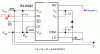
Please I have a very urgent problem. In the attachment is the set-up I used to test the IR21844S mosfet gate driver. Unfortunately, I have no outputs (on oscilloscope). Is there anything wrong with my set up? (NB: The diode is UF5406 (fast-recovery diode).
Thanks for your help.
Edwin
 

Attachments

  • Set-up for testing ir21844s.GIF
    Set-up for testing ir21844s.GIF
    7.6 KB · Views: 1,496
Even without the fets connected, I believe you should see pulses on the LO output.

What is the voltage of the SD pin? If its less than 0.8V then the chip is shut down.
Whats the voltage of your IN signal?
 
IR21844S gate driver: LO is ok but not HO

Hello jrz126 (very interesting picture you have there...),

Yes, in effect, I have a pulse at the LO output but nothing at the HO (just a straight 12V dc signal). However, I have just connected the Vs to ground and I have a square wave complementary to LO. Now I don't understand why I have to connect Vs to ground for the HO to work. I have not yet connected the driver to Mosfets but I will be using a full-bridge inverter (see image) so I thought I could use two gate drivers. As I will be using multi-level PWM, G1 and G4 will be complementary (G1-->HighOut; G4-->LowOut). G2 and G5 will be complementary also (G2-->HighOut; G5-->LowOut).
Will this configuration work with the IR21844S gate driver (and Vs connected to the corresponding floating Source of each leg)?
Thanks alot
Edwin
 

Attachments

  • full bridge.GIF
    full bridge.GIF
    5.3 KB · Views: 693
That pic is from "no-hands cat", its been my avatar since i joined the forum. too lazy to change it...

That configuration will work fine. I used the same driver chips when I built an H-Bridge for my inverted pendulum project.

**broken link removed**

How much power are you planning on running with it?

I am building a 3750VA inverter. Should work fine with the IRFP360 mosfets (23A rating).
But please I still don't see why I only have a square wave at the HO when Vs is tied to ground. In the H-bridge configuration, the High Mosfet is not tied to ground, and Vs as well. How will this work as you affirm?

Thanks alot.
Edwin
 
your test circuit is not emulating the actual use properly. With the setup that you have, the VS pin would need to be tied to ground in order for you to see any pulses on the HO pin. Tying the VS pin to ground in an actual application, though, will not drive the upper MOSFET, though - so don't do it.

The VB pin is the bias source for the upper gate driver. The VS pin is the reference for the upper gate driver. The diode and capacitor that are placed on those pins create a charge pump that allows the upper driver to have a bias that is referenced to the source of the upper FET since the upper FET does not have its source tied to ground. When the lower FET turns on, the VS pin is pulled low and the diode charges up the cap across VB and VS. When the lower FET is turned off, the flying capacitor is able to supply gate voltage to the gate-source of the upper MOSFET.

The driver circuit will work properly when connected to the bridge - just make sure you tie the VS pin to the proper node - see the datasheet.
 
You making a true-sine wave inverter? Or just a modified sine?

Yeah, I had the same problem when I first started playing around with these driver chips.
But like OutToLunch said, it has to be hooked up in the bridge for it to work.

At that power level, you're going to need a pretty good sized heatsink for those fets. I wonder if IGBTs would work better?
 
The VB pin is the bias source for the upper gate driver. The VS pin is the reference for the upper gate driver. The diode and capacitor that are placed on those pins create a charge pump that allows the upper driver to have a bias that is referenced to the source of the upper FET since the upper FET does not have its source tied to ground. When the lower FET turns on, the VS pin is pulled low and the diode charges up the cap across VB and VS. When the lower FET is turned off, the flying capacitor is able to supply gate voltage to the gate-source of the upper MOSFET.

Thanks, Out2Lunch, for the comprehensive explanation
Thread "threaded!"
Edwin
 
Status
Not open for further replies.

Latest threads

New Articles From Microcontroller Tips

Back
Top