Continue to Site

Welcome to our site!

Electro Tech is an online community (with over 170,000 members) who enjoy talking about and building electronic circuits, projects and gadgets. To participate you need to register. Registration is free. Click here to register now.

  • Welcome to our site! Electro Tech is an online community (with over 170,000 members) who enjoy talking about and building electronic circuits, projects and gadgets. To participate you need to register. Registration is free. Click here to register now.

Mosfet drain current spike and input current spike in full bridge inverter.

Status
Not open for further replies.

rashan shrestha

New Member
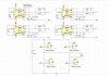
Hi everyone. I am currently trying to simulate a full bridge inverter using CPM2-1700-0045B mosfet and ADuM4121_4121-1 gate driver using unipolar switching method. I have a desired output current level and waveform along with desired voltage waveform and voltage level. however, I am seeing spikes in drain current(which is around 36 to 40 amps) in the high side mosfet of the bridge(whereas the peak drain current should be 12Amps-according to load and output voltage) when the low side mosfet is turning on( on leading edge) during which the high side mosfet is completely turned off( the PWM signal can show the if the mosfet is turned on or off). Similar is the case in the low side mosfets. I just cant figure out what is causing these current spikes in the mosfet. I have attached few images that will help get the idea of what I am doing.


The first four waveform shows the drain current for four mosfet of the bridge(AH1,AL1,BH2,BL2), the last two waveforms are the output voltage and current.
You can also see the PWM with the dead time in the next image.
The schematics of my simulation along with the gate driver unit is shown in the last image.

I would highly appreciate any discussions and solutions to this problem.

Thank you.

p1.JPG


p2.JPG


p3.JPG
 

Attachments

  • p3.JPG
    p3.JPG
    203.5 KB · Views: 235
  • p2.JPG
    p2.JPG
    190 KB · Views: 251
  • p1.JPG
    p1.JPG
    489.1 KB · Views: 257
  • p1.JPG
    p1.JPG
    489.1 KB · Views: 243
The current spikes do not appear to be travelling through R1, so the only other path for current spike is straight through both a high-side and low-side MOSFET. This is confirmed by the graphs showing that every HI and LO side MOSFET in a half-bridge pair have exactly the same spike at exactly the same time.

Therefore, it looks like shoot-through is happening every time you switch. This is happening because you are using the same signal to switch both MOSFETs in a half-bridge, but they often take longer to turn off than to turn on. That means that there is a brief time when both transistors are on and conducting to produce a short-circuit across the power rails.

Increasing Ron and/or decreasing Roff gate resistors should help because it makes the MOSFET turn on slower but turn off faster. The real solution is to control the MOSFETs independently and add dead-time so the signal to turn on a MOSFET is only sent after enough time has passed after a turn OFF signal was sent.
 
Last edited:
Could you please explain why the current spike happens and what has it got to do with roff. I changed roff value and the spike current is significantly less now. What other factors can high roff affect except obviously the switching speed.However, I want to keep the ron as less as possible for fast switching operation. The typical value of Ron for testing of the mosfet is 2.5ohms(from datesheet of the mosfet)
 
Could you please explain why the current spike happens and what has it got to do with roff. I changed roff value and the spike current is significantly less now. What other factors can high roff affect except obviously the switching speed.However, I want to keep the ron as less as possible for fast switching operation. The typical value of Ron for testing of the mosfet is 2.5ohms(from datesheet of the mosfet)

See my edited first post.
 
Last edited:
I do have a dead time implemented between two PWM pulses for the high and low mosfet(I have attached an image for that below).Also you were right the current spike is only during turn on time of the Low side mosfet( i.e high side drain mosfet current spike). I increased the Ron and the current spike decreased significantly, as a matter of fact what i found is the greater the difference between Ron and Roff, the lesser is the current spike.

p6.JPG
p5.JPG
 
I increased the Ron and the current spike decreased significantly, as a matter of fact what i found is the greater the difference between Ron and Roff, the lesser is the current spike.
That sounds about right. The larger Ron is relative to Roff, the lesser the spike should be because it causes the MOSFETs to turn on slower and turn off faster. If shoot-through is occurring even when you have dead-time, then you don't have enough dead-time.

In real life you would try and increase the dead-time just enough so shoot-through does not occur, which would allow you to minimize the gate resistors required so you can still switch on/off as fast as possible which reduces switching losses. You would then size the gate resistors just large enough to prevent issues like ringing, oscillations, and EMI. And then, since you now have gate resistances and the MOSFETs are switching slower, you might be able to decrease the dead-time one more time.

Trying to use gate resistances to prevent shoot-through instead of dead-time slows the MOSFET switching and causes the MOSFET To spend more time in the transition region where they are partially on/off and increases switching losses.
 
Last edited:
Your explanation is plausible. I was able to get my spike current from 36 Amps to 0.6 amps and I am still trying to reduce the spike to zero if possible. I wonder if there is a relation between the switching frequency and the current spikes.


p7.JPG
 
Your explanation is plausible. I was able to get my spike current from 36 Amps to 0.6 amps and I am still trying to reduce the spike to zero if possible. I wonder if there is a relation between the switching frequency and the current spikes.


View attachment 115113
Try doing what I said and set both Ron/Roff to zero, and then slowly increase the dead-time until shoot-through is zero. Then increase Ron/Roff until no ringing or oscillating occurs at the gate pin. Then decrease deadtime right up until shoot-through starts to occur.

Switching frequency is not so much the issue as switching speed (turn on/off ramp speed). It's just that as you increase switching frequency, you need faster switching speeds or else you will spend the entire cycle turning on or off rather than actually being on or off.

Any remaining current spikes that you see might be a result of turn on/off high frequency transients travelling through the parasitic source-drain capacitors of the MOSFETs. They are basically stick a tiny capacitor in series with the MOSFET that high frequency currents can travel through. Dead-time can't do anything about those. Only something that slows down turn on/off times like gate resistors can deal with that.
 
I was able to minimize the spike in positive half plane but the spike in the negative plane is still present. I tried increasing the deadband and it seems i cannot increase the deadband beyond certain limit at which the simulation stops working. I have tried various combinations of the Ron and Roff to get that negative spike down but its not working. do you know why this is happening?
 
is the negative spike lined up with the falling edge? show fewer cycles so there is more detail. We don't need to see so many.

I'm not sure why the simulation would stop working if the deadtime is increased too much. Maybe it doesn't like the floating nodes around R1 when all transistors are off.
 
the spike is linked up with falling edge of right half bridge(of high side mosfet) and rising edge of left half bridge(low side mosfet).

p10.JPG
 
I think your "gate drive" is slow. The turn on time is quite long. 2uS to charge up the gate to the turn on voltage.
Try slowing the switching frequency. Now you turn on the left side and as it turn on you are already turning on the right side.
I would go 1/10 the speed just to see how things work.
 
I am on my phone and can not see. Earler it looks like you turn on then in 4uS turn off. Then in 2uS turn the the orher side on. There is a 2 to 3uS delay for turn on. The gate drive is so slow you are having trouble. Please try slower. (Turn on for 40uS, then off)
 
I have been trying with the different frequency fron 2KHz to 20KHz but the is still the problem of vershoot. I am using the ADuM4121 gate driver. if you know some faster gate driver let me know. or how to make the same driver speed up to avoid the overshoot.
 
Status
Not open for further replies.

Latest threads

New Articles From Microcontroller Tips

Back
Top