Continue to Site

Welcome to our site!

Electro Tech is an online community (with over 170,000 members) who enjoy talking about and building electronic circuits, projects and gadgets. To participate you need to register. Registration is free. Click here to register now.

  • Welcome to our site! Electro Tech is an online community (with over 170,000 members) who enjoy talking about and building electronic circuits, projects and gadgets. To participate you need to register. Registration is free. Click here to register now.

Modify amplifier output

Status
Not open for further replies.

Micas

New Member
I wonder what to do to use a complementary pair of transistors (2SA1493 and 2SC5200) in the output of this amplifier (attached image) increasing the supply voltage to + -52V.
sqa2100_original_A.png
 
What you have to do is this:
- Calculate currently biasing for every transistor.
- Calculate resistors values so that the transistors get biased with the new voltage.
- Check that all resistors rated wattage with new voltage.
- You'll probably need to replace mot of the other transistors so that they can handle the new voltage level (haven't read into BC547/546 spec's so I can't say if they will last or not).
- Make sure that capacitors withstand maximum voltage.
 
The original amplifier with a +-25V supply produces about 40V p-p which is 14.14V RMS which is about 50W into a 4 ohm load. The amplifier is class-AB so which is about 60% efficient then the total heating of both output transistors is about 40W or 20W each which is fine.
When the supply is increased to +-52V then the amplifier output is about 92V p-p which is 32.5V RMS which is about 265W into a 4 ohm load. The heating in both output transistors will be a total of about 175W which is 87.5W for each output transistor and they will melt unless you cooled them with a huge heatsink, a high velocity fan and maybe some liquid nitrogen. The driver transistors will also get too hot and the circuit will need to be re-designed to supply the very high current. For such high output power amplifiers use paralleled output transistors.

AG, an eight Ohm speaker is shown on the schematic, rather than four Ohms.:)

Allowing a 5V supply line overhead:

Original amplifier with +-25V supply lines = 25W RMS

Proposed amplifier with +- 52V supply lines = 138W RMS

spec
 
Last edited:
The original amplifier design is pretty standard: voltage difference amplifier (VDA) (Q1, Q2) → voltage amplification stage (VAS) (Q4, Q5) → VBE multiplier (Q14) → current amplifier (Q8, Q10, Q12 & Q9, Q11, Q13) with current limiting (Q6 & Q7).

But there are a couple of problems with the schematic:
(1) As RonSimpson implies in post#3, Q13 should read MJ2955 (PNP), rather than 2N3055 (NPN)
(2) As AnalogKid implies in post #5, R34 and R35 should be swapped and the base of Q13 should connect to Q11 collector.
(3) There is also an omission: Q6, Q7, Q8, Q9 types are not specified. They are probably BC546/BC556 as used elsewhere on the amplifier.
(4) The junction of C17 and C18 should connect to 0V (ground)

Alternatively to (1) and (2) above, Q13 may in fact be a 2N3055, but on the schematic is shown as a PNP transistor and is drawn upside down.

spec
 
Last edited:
I wonder what to do to use a complementary pair of transistors (2SA1493 and 2SC5200) in the output of this amplifier (attached image) increasing the supply voltage to + -52V.

Hi Micas,

Welcome to ETO. I see you are from Brazil. Which area? If you put it next to 'Location' on your user page, it will display in the box at the left of your posts.:)

Interesting plan you have for your amplifier: it is just the sort of crazy thing I did when much younger, but can you tell us why you wish to increase the voltage of the amplifier power rails.

Can you also tell us a bit more about the amplifier: is it a HiFi amp, public address amp (PA), or perhaps a guitar amp.

What is the physical construction and layout- a picture would help.

My feeling is that you could increase the voltage of the power rails but, as the other members have implied, it would involve a lot of work and cost, and that is not to mention the much higher voltage and current power supply you would need. For example, all but three of the amplifier's transistors would need to be replaced and all but one of the capacitors.

So, my advise would be to simply build or buy a replacement higher power amplifier board. Amplifier kits and ready built amplifier boards are freely available and are reasonably priced on the net.:)

spec
 
Last edited:
Here are the modifications that would be required to convert the amplifier to +- 51V supply lines:

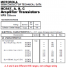
(1) TRANSISTORS (see post #8)
(1.1) An analysis shows that, with a reasonable heatsink and an 8 Ohm speaker load, the 2SC5200 and 2SA1493 transistors would be able to handle +-52V power supplies to produce 138W RMS, with stabilized power lines. With typical music, the output transistors would have a relatively easy time.:)
(1.2) The two driver transistors, Q10 (2SC4171) and Q11 (2SA1930) would not need to be changed, but they would need to be mounted on small heat sinks
(1.3) Q14 (BC548) would not need to be changed, but Q14 body flat-face should be mounted in thermal contact with the output transistor heatsink, near to one of the output transistors.
(1.4) Q1 to Q7 (there is no Q3) would need to be 120VCo minimum transistors (2N6517 [NPN]), (2N6520 [PNP])
(1.5) Q4 and Q5 would benefit from small heatsinks.

(2) CAPACITORS
(2.1) C17 and C18, change to 60V working minimum, 4.7uF minimum, but both capacitors must be the same.
(2.2) C10, C11, C12, C15 change to 60V working minimum.
(2.3) C16 Unchanged
(2.4) All other capacitors, change to 120V working minimum.

(3) RESISTORS
(3.1) Change R47 to 13K
(3.2) Change R41 and R42 to 39K
(3.3) Change R24 and R27 to 470 Ohms

(4) SETTING UP
(4.1) When the revised amplifier is built, the quiescent current (Iq) flowing through the output transistors will needed to be set back to 20mA to 30mA by adjusting the potentiometer (variable resistor) (TP4). Once the amplifier has warmed up re-adjust Iq, if necessary.

And unless I have missed something, that is it.:)

spec
 
Last edited:
Here is the original amplifier schematic corrected.

2016_10_23_SQA2100_ORIGINAL_AUDIO_AMP_corrected_03.png

 
Last edited:
BC547's are available in diffo voltage ratings, BC547A, B and C.
Q13 which is pnp obviously isnt a 2n3055, however an MJ2955 is a complment to a 2n3055 and is worth considering.
 
BC547's are available in diffo voltage ratings, BC547A, B and C.
Absolutely not. A, B and C are hFE ranges, not voltage ratings. This is from the datasheet:
 

Attachments

  • BC547 A, B and C.png
    BC547 A, B and C.png
    33 KB · Views: 148
Status
Not open for further replies.

Latest threads

New Articles From Microcontroller Tips

Back
Top