Continue to Site

Welcome to our site!

Electro Tech is an online community (with over 170,000 members) who enjoy talking about and building electronic circuits, projects and gadgets. To participate you need to register. Registration is free. Click here to register now.

  • Welcome to our site! Electro Tech is an online community (with over 170,000 members) who enjoy talking about and building electronic circuits, projects and gadgets. To participate you need to register. Registration is free. Click here to register now.

MN3008 Analog Delay questions

Status
Not open for further replies.

Fluffyboii

Active Member
Today I was looking for PT2399 prices and I was not sure to go Chinese cheap IC market or buying local since I needed 3 of them for decent delay and local prices were too high but I didn't wanted to risk getting fakes from China. After my fruitless pursuit for ICs I was at my favourite electronic shop looking for other stuff and I told the seller that I found the PT2399 but I ended up not buying because it was bit expensive.

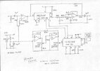
He told me he should have some and we checked but they were stuff similar with name like pt2249 or 53 but completely different ICs. Then I told him that it was for making delay and he said he had something like MN3008 at some where if that would do the job for me. I checked and saw that it was an analog delay chip and it was indeed used before for modular synth purposes. There were only two left because they were there for god knows how long. Apparently there were people getting in que to get one in the past. There were no MN3005 unfortunately. Anyway it looks like these were discontinued and they were sought after by DIY enthusiast. Anyone got some solid schematics for a delay module using two of these to get longer delay. I read that you need a clock and inverse of that clock. I got some inverter ICs like 4069, 40106 that I can use for getting that type of clock signal.

I am aware that PT2399 is a digital delay module and this one is analog so they will need completely different circuits in order to operate. Because MN3008 has half the stage count of MN3005 I want to use two chips I got in series to create a longer delay.
1663355078079.png

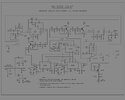
One main problem is that chip requires -15V. My power supply can give +/-12V. But it actually has something around +/-16.5V lowered to 12V with linear converters to get rid of ripple. So If I get 15V and -15V linear converters I can convert it to an +/-15V power supply. I am not sure those linear converters can operate with 1.5V headroom but I can also get a transformer with higher voltage out. But this would mean quite a lot of expenses and I don't want to mess up my other circuits working with 12V. Instead of that can I get the 16.5V DC and use a simple resistor divider or just directly feed it to the chip since its max operating voltage is -18V. I still have 14100uF filtering caps on both rails and load is rather low so I don't think it would suffer from voltage supply ripple. I can also add non electrolitic caps for uncoupling for being sure.
Voltage problem aside the MN3101 needs to be replaced. I found this in here:
1663355697848.png

It seems MN3008 needs a clock signal and same signals inverted version. I have CD40106 I used before for an oscillator and it looks like a good replacement since I can also invert the signal in the same chip. It would be sad to leave all other 4 not gates unused though. Looks like CD4047 is often used.
Also: "-A LFO for modulating the delay clock. This also requires some sort of circuit that allows the slowly varying voltage from the LFO to influence the timing of the delay clock. Once this is in place, the effect can go from being "just a delay" to also having flange/chorus/vibrato ability." I have an voltage controlled LFO. If I can use a VCO for the clock like CD4046 can I achieve those effects. Can I use an existing VCO based around CD40106 and just invert the output for clock. If I can I may just build a board to connect to me triple VCO (it even has 3 unused gates of the CD40106) and it would be awesome.

Edit: It turns out my transformer gives 17.5V out after rectification without load. I will need atleast a resistor divider. Or I can just try 12V and see if it works. Some folk said it worked for him. Does this thing only need negative supply? It may be more logical to get a -15V linear converter then. I wish buck converters didn't had the high frequency noise. They are terrible for audio use.
 
Last edited:
Look carefully at the circuit - they are operating it between 0V GND (as IC -VDD to pin 5) and V+ as IC GND to pin 1.
You do not need an actual negative supply, it's all relative.

Also the supply voltage vs gain graph just above that circuit in the datasheet shows it operating from between 8 to 16V.
12V should be fine!

The VGG voltage is important; that should be at about + 1/15th supply compared to the IC VDD pin, so with VDD pin grounded about 0.8V or so, as 1/15th of 12V. A resistive divider and small decoupling cap is probably enough. Fine tuning that can reduce distortion, so possibly using a preset to give 0.5 - 1V or so could be good?
Or use two series diode from 0V with the preset across the upper one and a pullup to V+ to 0.6 - 1.2V range?

It looks like you may be able to just parallel power and clock for two ICs, then connect the input of the second to either of the outputs of the first.
I see. Because I am very bad at designing analog circuits I don't want to makes something stupid and risk these chips but I will try to draw something and post it here if I can't find a schematic.
 
The VGG voltage is important; that should be at about + 1/15th supply compared to the IC VDD pin, so with VDD pin grounded about 0.8V or so, as 1/15th of 12V. A resistive divider and small decoupling cap is probably enough. Fine tuning that can reduce distortion, so possibly using a preset to give 0.5 - 1V or so could be good?
Or use two series diode from 0V with the preset across the upper one and a pullup to V+ to 0.6 - 1.2V range?
Now I understand what you mean. Normally they use MN3101 for clock since it is conveniently also supplying the Vgg voltage. Looks like as you said a simple resistor divider should do the job with a fine tuning trimpot that can change the voltage slightly.

1663439923678.png

I was checking this circuit to understand how it works. I am not sure how the CD4046 PLL works but op amps seems to be just increasing the input level. My circuits are operating with signals lower than 10V peak to peak. I also heard that I can just use a 555 chip to drive a dual flip flop to get a drive signal and its inverted version but I don't have the said flip flop IC. It looks like I can just replace the op amp with LM741 and change the resistor values for my needs. I will breadboard that and experiment to see if I can get a clean square wave and its inverted version.

I also looked about NE570 for decreasing noise in BBD circuits. It is a compander and expander but it looks like it is also an old chip that is hard to find. I found an op amp based compander circuit but getting it expanded back without much distortion and fully denying compander effect seems to be another challenge by itself. So it carries second priority sice it can be added after I confirm the operation of the circuit.
 
Last edited:
That opamp circuit is a bit strange - It is to offset the voltage because the PLL is operating on a negative supply, in that circuit; pin 16 (Normally power) to ground and pin 8 (normally ground) to -14V..

To have everything operating between 0V and +12V, you should not need that; just use a pot across 0V and +12V to start with, with the wiper to 4046 pin 9, and see what actual voltage range you need for the delay range you want.

Once you know that, it should be easy to work out a simple opamp circuit.

The NE570 was a brilliant IC, I used a few of those in Amateur Radio voice compressors back when I was active on voice instead of digital.

I still have one in an old box of analog ICs - just right of centre, 1990 vintage:

Analog_ICs_sm.jpg
 
That opamp circuit is a bit strange - It is to offset the voltage because the PLL is operating on a negative supply, in that circuit; pin 16 (Normally power) to ground and pin 8 (normally ground) to -14V..

To have everything operating between 0V and +12V, you should not need that; just use a pot across 0V and +12V to start with, with the wiper to 4046 pin 9, and see what actual voltage range you need for the delay range you want.

Once you know that, it should be easy to work out a simple opamp circuit.

The NE570 was a brilliant IC, I used a few of those in Amateur Radio voice compressors back when I was active on voice instead of digital.
Because I am using a dual lane power supply it should be possible to connect the negative rail to MN3008 and positive to PLL. But I don't need one and I can just connect the power connections in reverse the get relative negative voltage, right? I will check the clock speed according to voltage for the CD4046.

It is bit of a shame that I was born in era of digital and can't find some analog ICs.
 
Last edited:
To have everything operating between 0V and +12V, you should not need that; just use a pot across 0V and +12V to start with, with the wiper to 4046 pin 9, and see what actual voltage range you need for the delay range you want.

Once you know that, it should be easy to work out a simple opamp circuit.
I set up the CD4046 as a clock with inverted outputs like the schematic above did and it worked as it supposed to. I assume maximum delay is achieved with slowest clock the BBD chip can handle which is 10Hz. What happens if we go slower, does it explode or we get aliasing effect. Edit: it was supposed to be 10khz :/


The PLL VCO doesn't work under 1V so I set it as a way that it will get to 10Hz at 1.2V and it will go a bit slower around 5Hz if I turn the middle frequency range pot. It goes up to 7.5khz if CV is 12V and resistance is at minimum. Since max it will get at CV input is 10V, max frequency reduces to 7.15Khz. I think I need an op amp to sum 1V with the CV signal so that it will always oscillate or set a resistor divider. Do I really need Op Amp buffering here though.
1663455577415.png

It looks like higher clock speeds are used for creating a effect called flanger so any ideas how I can get a wider bandwidth out of the CD4046. One possible way would be adding a capacitor in parallel with the existing one via a switch for slower clock speed and change the default cap to something smaller.
Edit: Ignore the values since they are wrong.
??
It is nice that it is currently purchasable but what I was talking about about general lack of old analog chips that are mostly replaced by microcontrollers, not only the NE570. Finding LM13700 is also difficult since DIP version was discontinued and finding MN3005 is apparently not possible without going through possible fakes or paying high prices. Who knows what will happen after 2 decades or so. I can't buy from Ebay because of meaningless tax amounts and shipping cost over 20USD. I bought ICs from Aliexpress with mostly good luck though (except AD633 and TL07x stuff that have bad slew rate and such but still usable in most cases). I am very very sure that the local shop here buys their LM13700s from there since the one I got is exactly same with the ones that came there lol.
 
Last edited:
I randomly found this schematic on google images. I can't find info about it but looks decent to start with.
Ok found more info: http://www.hollis.co.uk/john/circuits.html
Looks like this circuit is for small delays. And when you want to squeeze the maximum delay from a single chip performance drops and problems like oscillator clicking noise leaking become more noticable. This just seems and feels like my ring modulator misery. Can't wait to build it and see what happens when I increase the cap size. I will need to check the values and connections before putting any mn3008 in it though.
 

Attachments

  • images (6).jpeg
    images (6).jpeg
    31 KB · Views: 284
Last edited:
There is anothet schematic with dual BBDs. I think I can use the clock from the other one in this one. I dunno why they chose to use transistor filters though instead of throwing more op amps to it. I honestly don't care how many op amps it will need so maybe I should replace them with op amp filters.
 

Attachments

  • IMG_20220918_162202.jpg
    IMG_20220918_162202.jpg
    176.3 KB · Views: 304
1663540430771.png

rjenkinsgb. This is what I came up with. It works between 7Khz and 60Khz. The added reference can be adjusted with a trimmer to get exact 10Khz at low end and I can always put a switch and another cap to get higher frequency mode but I think it is a good start. I am not sure how linear this will be according to CV. I think using inverting summing configuration and just using another op amp to invert it back can be more reliable and I should not cheap out on this since MN3008 is the most valuable IC I have.
I tried adding a resistor to R2 but it made the range very small since it determines the lower clock speed limit but it also makes it go faster. Capacitor can be increased in size to fix that but I think it is just not needed.

Also does BDD work with positive clock voltages. CD4046 gives out positive pulses. Datasheet says max high clock level should be -1V low should be Vdd but the schematics just connects outputs to the BBD.

1663550109964.png


This would be more reliable I think. I did not test it yet though.
 
Last edited:
rjenkinsgb Are you sure about that the BBD requires 1/15th of the input voltage. I read somewhere that gate supply voltage should be around 14/15th of the input signal instead. The final circuit I posted just uses MN3102 Vgg output since that IC already supplies the reference voltage by its inner Vgg power supply. Only thing I don't really understand is the 4148 diode in there. I assume it is there to be sure that voltage of the MN3102 is bit lower than the MN3008 so that it will never be able to give full 12V into the chip since datasheet states Vgg should be typically 1 volt more than the Vdd.
1663696616754.png

The other circuit again uses a 8.2 zener for the low voltage BD3208 chips which operate at 9V and 8.2V is again 14/15 of 9V.
1663697214768.png

I just realised that I got the wrong chip. I should got the MN3101 instead of the MN3102. Such a shame tbh.
 
Are you sure about that the BBD requires 1/15th of the input voltage. I read somewhere that gate supply voltage should be around 14/15th of the input signal instead.
It's 14/15 of the supply when operating on 0V and -15V, where VDD is at -15, making VGG about -14V

For operation on +12V, VDD is 0V and VGG should be somewhere around 0.8V

If you look at the graph "Vi-Gi" in the data sheet, the amount of distortion appears to depend on the exact VGG voltage, so I'd make it adjustable over a small range to see what effect it has?
Sure. Just all of the schematics directly use the MN3101 or 3102 Vgg power supply pin. Maybe it auto adjust internally for minimum distortion. I will find MN3101 first, probably the same shop I got the MN3008 and MN3102 has it too. Worst case scenario I will buy it with the SA571 from China and see what it will be like.
 
I placed an order for the missing parts. Now I will wait. I am planning on building this one with only 2x MN3008s. I tried finding another MN3008s but there are none without paying outrageous prices. At that point I would just buy like five PT2399 chips and go with the digital way.

1663705582430.png

Does anyone know the difference between 2SC1815GR and 2SC1815BL. At the store we checked the listings and couldn't find a meaningful difference so I just bought 6X 2SC1815GR instead.
There is a screenshot from PDF if you don't want to download it:
1663705948115.png
 

Attachments

  • AD-900_MN3008_Version_Build_Document.pdf
    1.9 MB · Views: 235
Last edited:
That's the gain category. GR has Hfe in the 200 - 400 range, BL has it in the 350 - 700 range.
Wow thats is a lot. I guess I better find those as well. Or just try and see what happens when I don't. I asked my school collab space about making the pcb in the PDF file and teacher said that it should be possible to make one. So I can just solder it like a kit. Except that I don't have 4 MN3008s. It looks like I can just leave unpopulated those extra components in their places, just solder Q6 and Q7 and bridge C20 to Q2 with a temp wire in case I find more BBD delay chips in the future and double the delay.

My transistor tester tells me the Beta value of the 1815s is around 330. I guess high gain of the other version makes them more suitable as filtering amplifiers. I wish they just used op amps but I guess I will just get the correct ones. I can buy 1845 instead online. It looks like it is a version with higher voltage and current capability and beta is typically 600.
 
Last edited:
Status
Not open for further replies.

Latest threads

New Articles From Microcontroller Tips

Back
Top