Continue to Site

Welcome to our site!

Electro Tech is an online community (with over 170,000 members) who enjoy talking about and building electronic circuits, projects and gadgets. To participate you need to register. Registration is free. Click here to register now.

  • Welcome to our site! Electro Tech is an online community (with over 170,000 members) who enjoy talking about and building electronic circuits, projects and gadgets. To participate you need to register. Registration is free. Click here to register now.

Maximum RFI suppression needed for this circuit

Status
Not open for further replies.

DDT

New Member
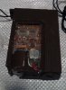
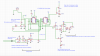
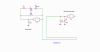
The following circuits show the original and the updated version of the input section of a break wire alarm. The sensor is a 20m long twisted wire 0.1mm, which activates the alarm when broken. The wire keeps the logic input low and when it opens the logic input goes high. The first priority in designing this circuit was maximum robustness against false alarm due to RFI and other induced noises, and also low power consumption as it's powered by a 9V battery. Although the protection seems to be enough I'd like your input regarding the value of chosen capacitors and whether they are all necessary. Additionally, other suggestions regarding the design of PCB will be welcomed.The PCB is a regular two layer type with copper plane assigned as the ground.

Kindest regards
D
 

Attachments

  • Sesnsor input.png
    Sesnsor input.png
    46.5 KB · Views: 262
  • Sensor input 2.png
    Sensor input 2.png
    73.7 KB · Views: 258
PCB:
I would not run the "input" traces across the board! Keep those traces very short.
(Input connector at edge of board. connect to inductor with short thin traces. Connect to R100 ohm resistors with thin traces.)
All the above with out a ground plane, top or bottom side and no traces on the other side of the board. Some people will say to use a ground plane but I would not. I am thinking of high voltage from lightning. (RF and high voltage) I don't want that to get onto the ground.
Now turn on ground plane on top and bottom. C6 & C8 very close to the 100 ohm resistor. Use wide traces.
Next the rest if the caps. You want to kill the RF and high voltage spikes at this point not across the PCB.
C11, R8 I would put at the CMOS logic.
Every one will have a different idea. Read their logic.
 
You should include a common mode choke at your input, preferably at a physical position that prevents RF coupling onto your board. The obvious location on the schematic would be to the left of R11 and R12. Your sensor wire, at 20m long, will be a good antenna for frequencies ranging from 1MHz to 500MHz and beyond, so you have to provide suppression that is effective over this broad frequency range. C7 and C10 are both critical for this. I think that C6 is also useful to extend the bandwidth of bypassing beyond what C7 can provide. C8 seems not that useful unless it is intended to be placed right beside TVS1 and act as its bypass, but with proper placement C7 and C6 should do that job. C9 and C10 are a bit redundant and assuming the component placement is very close, you could change C9 to 100 pF. I might also suggest that a 100 pF cap across D1 is a good idea to prevent rectification of any RF that gets that far. Is there really any point in including D1, by the way?

I wonder if the resistance of R4 is a bit high to be practical. If this is an outdoor application, you should expect some leakage between your sensor terminals due to humidity or other moisture and with such leakage, you will get a false alarm.
 
  • Like
Reactions: DDT
I might also suggest that a 100 pF cap across D1 is a good idea to prevent rectification of any RF that gets that far.
Like connecting the cathode of D1 to left side of R8? I think the D1 is there to block ESD. I thought C8 would be useful as it's 1nF i.e. midpoint of 100pF and 10nF to cover this frequency range. What do you think about these new type of capacitors called X2Y, they are supposed to be more effective than MLCCs? Regarding the leakage, the circuit board will be potted and placed inside a waterproof aluminium case, so I don't think the moisture would be an issue.
Kindest regards
D
 
Last edited:
Looks like overkill. I don't see any need for D1/TVS1, and most caps wouldn't be required. Some resistors in series with the loop and a capacitor in place of TVS1 would be enough. Resistors of 10K, and a ceramic capacitor of 1uF will have an attenuation of 100dB @ 1MHz. Passing the twisted pair through a ferrite bead a few times will give more protection that you may or may not need.
 
Resistors of 10K, and a ceramic capacitor of 1uF will have an attenuation of 100dB @ 1MHz.

Which resistor you'r referring to? Using only a 1uF capacitor wouldn't cover very high frequency such as those from cellphones. Regarding the type of capacitor itself, I've found image of similar device which I think is a military device (Russian). The silver cube is a polyethylene film capacitor к73п-3, 50nF.Do film capacitors perform better than ceramic in this type of application?
 

Attachments

  • 3887627.jpg
    3887627.jpg
    374.4 KB · Views: 226
Sensor input 2.png
R4,R8,C2,C11 : evt.power-ON the caps short digital input to GND and dev. I.D1(R11+R12)+U.D1+U.wire=U.x at anode of D1 , evt.wire-Break the C2 will be charged from U.x to U.th and on to U.cc
... !perhaps? add a ferrite bead over the c11 or incase it's an smd ?? 10k series resistor in parallel with forward low capacity diode
 
Film capacitors have a better Dissipation Factor due to their dielectric. But for bypassing NPO/COG dielectrics are fine. Size will matter for RFI to reduce parasitic resonances. Ferrite beads are your friend w.r.t. such. Choose ferrite beads for different freq ranges as well as they have limited range use. Twisted pair CAT6 is a good idea.

Once you start to go past 500Mhz things start to get sensitive and ball parking parts might not be enough.
 
Once you start to go past 500Mhz things start to get sensitive and ball parking parts might not be enough.

What frequency range this device would be more sensitive to i.e which frequency is more likely to cause false alarm?
 
That depends on the bandwidth of the CMOS sense circuitry. My preference would be to lower the impedance of the input to perhaps 1K or so using a burden resistor plus a common mode choke and dual (both input lines) ceramic capacitor bypass to chassis earth, not supply ground. a TVS is unnecessary unless you expect some heavy EMI from a motor or electronic lighting ballast .

Edit: this would require a pull up resistor of 500Ω or so to trigger the CMOS. This places a 6mA drain on the supply. Not an issue unless it's battery operated.

If it is battery operated, I'd probably do the same, but use a 1% duty cycle pulsed squarewave to verify the continuity and lower power drain.
 
Last edited:
If it is battery operated....

Thanks for the suggestions. I'd appreciate it if you could show me schematically. The circuit is battery operated and it should operate at least 2 weeks on 9V battery (3x3V lithium). The complete circuit is attached for more clarification.
 

Attachments

  • FALRE TRIPWIRE.png
    FALRE TRIPWIRE.png
    256.8 KB · Views: 212
Have a look at this for an oscillator with adj duty cycle.
**broken link removed**
Just feed the output along the sense wire and monitor it with a spare schmitt trigger, comparing the source and received signals biased in favour of the received signal to enable triggering when that signal is lost. You can isolate the incoming signal with a DC blocking capacitor to permit DC bias Adjustment from sensitivity control, which will also handle any false triggering issues.
 
  • Like
Reactions: DDT
comparing the source and received signals biased in favour of the received signal to enable
Would you please explain this more. I understand the part about generating adj duty cycle pulse using a schmidt trigger NAND, which by the way is excellent as it uses the same IC as in the circuit, but I don't get the part about comparing and triggering signal.
 
Ok , I was thinking in terms of an OPA schmitt trigger...in this case the single input 4093 trigger has an established logic level reference already. So the approach would be a small (say 10nF) cap and perhaps a 100K variable resistor in parallel with it at the input of the monitoring schmitt trigger. The pulse train will 'charge' the 10nF cap and activate the monitoring schmitt trigger. Loss of the pulse train will discharge the 10nF cap and deactivate the monitoring schmitt trigger. Adjusting the pulse train duty and the variable resistor across the 10nF cap will control the overall time constant of the system response and pretty much eliminate electrical interference issues. With this arrangement no 1k burden resistor or pullup is needed. The oscillator provides the pullup.
 
  • Like
Reactions: DDT
Ok , I was thinking in terms of an OPA schmitt trigger...in this case the single input 4093 trigger has an established logic level reference already. So the approach would be a small (say 10nF) cap and perhaps a 100K variable resistor in parallel with it at the input of the monitoring schmitt trigger. The pulse train will 'charge' the 10nF cap and activate the monitoring schmitt trigger. Loss of the pulse train will discharge the 10nF cap and deactivate the monitoring schmitt trigger. Adjusting the pulse train duty and the variable resistor across the 10nF cap will control the overall time constant of the system response and pretty much eliminate electrical interference issues. With this arrangement no 1k burden resistor or pullup is needed. The oscillator provides the pullup.

Thanks, it makes sense now. The filtering components will not applicable though as they will be interfering with charge/discharge cycle. Maybe a diode before the monitoring components?
 
What charge/discharge cycle?
Consider the monitoring schmidt trigger with 10nF cap and 100k variable resistor at its input, wouldn't the inclusion of other filtering components such as capacitor between the oscillator and monitoring trigger change the behaviour of 10nF cap i.e changing the RC time constant? looking at the break-wire between point A and B (attached image of your suggested circuit), does the circuit benefit from filtering components at all?

P.S C2 should be 10nF as you suggested.
 

Attachments

  • OSC.png
    OSC.png
    129.3 KB · Views: 210
It will work in both instances, but the TC will change and you just adj. the variable resistor to suit. Try it w/o any decoupling caps as per your schematic. The only advantage to decoupling series caps is DC isolation for the exposed breakwire. If the likelihood of accidentally DC getting into that wire is low, no decoupling caps are required.
 
  • Like
Reactions: DDT
It will work in both instances, but the TC will change and you just adj. the variable resistor to suit. Try it w/o any decoupling caps.
OK great, so if you were to compare the oscillator circuit in my last post with the original circuit, how would you rate them each from 1 to 10? I never asked, but what is it about this oscillator circuit that makes it more immune?
 
Status
Not open for further replies.

Latest threads

New Articles From Microcontroller Tips

Back
Top