Continue to Site

Welcome to our site!

Electro Tech is an online community (with over 170,000 members) who enjoy talking about and building electronic circuits, projects and gadgets. To participate you need to register. Registration is free. Click here to register now.

  • Welcome to our site! Electro Tech is an online community (with over 170,000 members) who enjoy talking about and building electronic circuits, projects and gadgets. To participate you need to register. Registration is free. Click here to register now.

Making a little daughter PCB look like a SOIC8...(the legs)

Status
Not open for further replies.

Flyback

Well-Known Member
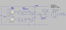
If i may please ask....We are doing a 2kW SMPS. PFC then Half Bridge LLC.

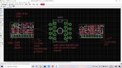
The main board has the chunky components on it and is rather large for this initial prototype (500mm x 400mm).

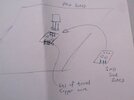
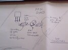
Therefore, we dare not put SMD on this potentially ‘bendy’ board. Though we need the Gate drive components to be SMD for sake of reducing stray L. As such, do you think the attached method is good for doing the gate drive with SMD daughter boards?

Its basically making the daughter board into a little kind of SMD component. (As SMD, The daughter board will be easier to remove if we need to, during testing.)

BTW, the cheap Chinese PCB Fabs don’t seem to be doing >1.6mm thickness on the cheap rates for our main board size, so we must use 1.6mm thick main board.

The below is the only thing I can find so far, but we need the legs to come “out” so we can solder them to the mains board SMD pads…..
https://uk.farnell.com/wurth-elektronik/61000418221/header-2-54mm-pin-smt-4way/dp/2356209

Is there such “SMD header” as in the attached picture? Basically we just want a header which will kind of put "legs" onto the daughter PCB.....to make it kind of like a SOIC8, type of thing...those kind of SMD "legs"

I mean, the below could kind of be hacked to do it..
https://uk.farnell.com/multicomp/mc34747/header-1-row-r-angle-3way/dp/1593427
....but its going to be a bit "raised" compared to a SOIC, kind of thing.
 

Attachments

  • LLC gate drive.jpg
    LLC gate drive.jpg
    163.9 KB · Views: 214
  • Gate drive layout.jpg
    Gate drive layout.jpg
    63.6 KB · Views: 213
Last edited:
The conventional (and simplest) way of adding small sub-PCBs is to position them vertically and use SIL pins or connectors.
They are used both for PCB subassemblies and thick film modules.

eg. This type of style - the red or black modules. The six upper left ones on this board are part of a three phase power driver, as it happens:

FANUC-A20B-0009-0320-Control-P-C-B-DC-axis-drive-board-fitted-on-FANUC-servo.jpg_Q90.jpg_.webp
 
Thanks, sorry i should have said, this gate drive is for LLC and can go up to 250kHz. I wonder about SIL pins for that?
 
Through hole components have been used for many years without problems at 500+ MHz.

250KHz is nothing.
 
Thanks, yes, i appreciate...AYK, Thru hole is soldered, rather than the extra "flimsiness" of a connector, involving contact surfaces possibly lying "lazily" against each other. AYK, unsoldered surfaces have in fact minimal contact, at the microscopic level......it is a bit of a worry for a gate drive with high rise time, and very high fall time......its sub 100ns tf and tr as you know.
 
You can solder them if required; they often are in production equipment.
Just use a right-angle pin header on the sub board and a SIL pattern on the mainboard.

The gate current will be controlled by the series resistor on the output of the driver, which also damps any parasitic inductance in the connection from there through to the device gate.

Is it more than 2A? Any decent pin socket should take that for testing & prototyping.
 
Thanks, its less than 2A.

As you kindly recommend, i could use this on the sub board....
[1]...
...and then this socket on the main board...
[2]...
....do you think that would be ok for the 250kHz, <100ns tr signal?

I could double up the connections so as to be sure the gate drive current definetely gets through?

We dont wish to solder the header into the main board, as with some of them with multiple ways, it will be a devil to remove if we need to.......however, if it was surface mount then it wouldnt be so bad........i'm still a bIt worried about [1] connected to [2] above
 
Last edited:
I'd put doubling up power and ground as the most important. If you are using a two row header, you could make one row nothing but ground and power.
 
You could design the daughter board with castellated holes, then it can be soldered to the main board like an SMD component. I believe this gets around your objections and meets your goals. This video gives you all the details about castellated boards.

ebd30f240f94d8e32dbd8ddcf1e12c0845d0ca3a.jpeg


But, you object, this raises the price to have the boards made at Chinese fab houses. Yes, it does, but it saves a ton of messing about. But there's a secret to greatly reduce the per-board cost. The Chinese fabs charge little or nothing to panelize a board with v-scoring as long as it's a single design per board. If you castellate two edges, lay out the panel with routed space between the castellated edges with v-scores between the other edges.

I recently designed a small pcb with a watchdog timer circuit that hangs off a PIC ISCP connector. Why pay $5 for 10 boards when I could get 200 for the same price??? (Ten would probably be all I'll ever need, but it seems like a handy thing to have.)

20220511_100612.jpg
 
Thanks, i like castellated holes...especially for production.....though in testing, when we may have to remove and replace the board multiple times, i wonder if the castellated pads will be removed from the board...

I'm actually now thinking of the single line SIL header.....and indeed soldering this into the board, into PTH ....and just being very careful when i remove it from the board.......desoldering it and "micrometer pulling" it bit by bit, till its removed, so that i dont damage the pads......i believe PTH pads are less likely to be pulled off during desoldering than SMD pads.

Best of all would be the SIL header to SIL housing...then it just pulls apart...but goodness only knows what that will do to fast rise time (<100ns) gate drive signals at 250kHz. Maybe we can put in the footprint for the SIL housing, and if it doesnt work.....remove the housing and solder the header pins direct , as Many of you have kindly suggested, including RjenkinsGB's greatly appreciated suggestions.
 
Hi,
As we all know, if you have an SMPS on a big main board, which comprises heavy components, then you cant put SMD on it, as it will crack or go open when the main board flexes…so , for prototyping only, what about the attached method to get SMD on to a big main SMPS board?

Its just a little PCB, with SMD components on it…..and it has thru holes which line up with holes on the main PCB, and little bits of tinned copper wire are pushed through these holes to solder the little SMD PCB to the main board.

....there aren't even any "sticking out legs", so lead inductances will be to a minimum, which is good for things like gate drive componentry and current sense circuitry etc.

Do you see any problems with this?
 

Attachments

  • Little bit of PCB on main PCB.jpg
    Little bit of PCB on main PCB.jpg
    51.4 KB · Views: 193
You could use right angle header pins of either 0.1" pitch or 2mm pitch for a more compact and lighter alternative.

SmartSelect_20220512-165758_Edge.jpg
 
Those are exactly what I originally suggested, but he seems to think a few MHz needs microwave design rules...
 
Definitely not my area of expertise, but the stated solution doesn't seem to be very workable:

"Its just a little PCB, with SMD components on it…..and it has thru holes which line up with holes on the main PCB, and little bits of tinned copper wire are pushed through these holes to solder the little SMD PCB to the main board."

In the words of EEVBlog Dave, the "little wires" are going to leave the daughter board flapping around in the breeze.
 
In the words of EEVBlog Dave, the "little wires" are going to leave the daughter board flapping around in the breeze.
Thanks, the jdea was to do two 0.3mm vias, and then stitch thin tinned copper wire through both, and twist it tight on one side, so it doesnt flap about too much.....however, i actually like its looseness of connection, as it wont be too mechanically coupled to the main board, ....whose flexion stress is the reason for doing the sub board in the first place.....this is only for prototype...not for prod.....in prod, the boards will definetely use headers and be vertical......vertical boards, AYK, are a bit more awkward for tweaking components on them....and we dont like non soldered connections for eg gate drives.

Also, i need the SMD layout to be tight to the fets being driven........
 
You can also put the driver and control pcb on the bottom side of the power board, have it screwed in and just run vertical connector to each of the mosfets.
 
Flyback, Not certain what you are doing but here is a picture.
I am using three small pins in a PCB to go into sockets in the big PCB. The sockets are inside the PCB so they take up about as much room as a VIA. The parts are on the bottom side the small PCB. Current is about 4.5A peak. Very fast edges.
1652470028309.png
 
You can also put the driver and control pcb on the bottom side of the power board, have it screwed in and just run vertical connector to each of the mosfets.
not sure if I made myself clear enough, the two pcbs are parallel with an isolating shim between and standoffs maintaining rigidity. Power pcb with thick copper, control pcb with fine traces and smds. I did mines single sided mount with lots of testpoints like this https://www.aliexpress.com/item/32831872442.html for easy testing and modification. But mind you it is a heavily overengineered welder inverter with little to none expense spared in hopes of reliability and easy testing, not a production kind of thing.
 
Last edited:
and oldish 3D mockup in solidworks
(the 3D PDF most likely works in Adobe reader only)
 

Attachments

  • main.PDF
    287.8 KB · Views: 224
So, We are doing 2Kw LLC Half bridge with vin = 400vdc.
The hi side drives are (on the prototype) being done as in the attached. The little sub-boards allow us to use SMD components without risk of them suffering possible flexion stress, which they would get if they were on the big main board.
Do you think this single SIL connection will stop flexion on the main board from occurring to the sub board?.....the header will be soldered into the main board

(also attached is an LTspice of this gate drive)
 

Attachments

  • Gate drive layout_hi side.jpg
    Gate drive layout_hi side.jpg
    420.9 KB · Views: 201
  • Gate drive cct_hi side.jpg
    Gate drive cct_hi side.jpg
    149.6 KB · Views: 192
  • LLC with chosen gate drive transformer.asc
    16.6 KB · Views: 191
Status
Not open for further replies.

Latest threads

New Articles From Microcontroller Tips

Back
Top