Continue to Site

Welcome to our site!

Electro Tech is an online community (with over 170,000 members) who enjoy talking about and building electronic circuits, projects and gadgets. To participate you need to register. Registration is free. Click here to register now.

  • Welcome to our site! Electro Tech is an online community (with over 170,000 members) who enjoy talking about and building electronic circuits, projects and gadgets. To participate you need to register. Registration is free. Click here to register now.

Low noise TEC driver design - adjustable linear voltage regulator

mk795

New Member
Hi all,

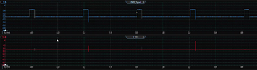
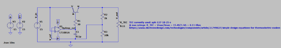
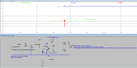
I currently have a project where I want to heat a EMI sensitive device (DUT) with a peltier module. I started with an Arduino, a MOSFET driver module (IRF520N), a lab power supply, a temperature sensor attached to the hot side of the peltier-element (TEC) and a Peltier module with the ratings (Imax = 1.9 A, Vmax=15.4 V). The system is PID controlled. During heating, the DUT was not probperly working anymore. I observed voltage peaks in the voltage after the MOSFET driver that are synchronized with the negative edge (switch off) of the PWM signal. Those are likely the interferences disturbing the DUT too much.
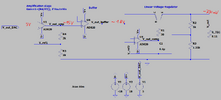
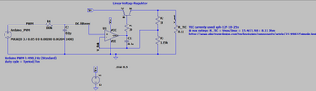
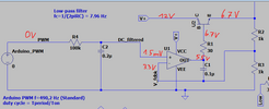
So what I require is a low ripple (unfortunatly, I am not able to specify a specific ripple value) smooth DC voltage driving the TEC. I thought about a linear voltage regulator circuit. In addition, I need to be able to adjust the voltage in a range of 0 to 15 V (at the best with the Arduino). So, I came up with the circuit attached. I plan to convert the PWM signal with a DAC to a signal adjustable from 0 to 5 V. Then I want to amplify this signal and make it the input of my voltage regulator circuit. Unfortunatly, I am not able to deliver the 15 V. I thought the buffer might help, but I would need a resistance in series with the buffer output of at least 300 Ohm (acc. to the simulation) to get a 15 V buffer output. But still, when connecting to the non-inverting input of the third op amp, it is not working.

I am (clearly) not an expert in electronics and I would be very happy about any tipps and tricks, to make my project work. Thank you!
 

Attachments

  • Peaks_PWM.png
    Peaks_PWM.png
    547.9 KB · Views: 94
  • TEC-driver_circuit.PNG
    TEC-driver_circuit.PNG
    43.6 KB · Views: 99
There are many mistakes in your design.
  1. Stage 1 has excess gain and is redundant
  2. Stage 2 is redundant.
  3. Stage 3 cannot barely drive 30 Ohms+ hFE * 8Ohms since the Op Amp is current limited.
  4. NPN collector cannot draw current from Stage 2 .
    • Connect NPN-C to 15V
  5. R3 is now too big,change to 500 or 470, Av=3
  6. When NPN-E is V+/2 both 8 ohms and NPN are dissipating equal power ~ 7 W linear
  7. Where and why is there PWM? (DUT or Peltier?)
  8. How is heat shared with DUT? Show pix.
1707333460154.png


Make the necessary changes after you answer 7 & 8.

I suggest using Power transistor or FET onto heatsink with DUT to raise junction temp and use that instead for heater with emitter to Re=? as a current sensor grounded.
 
Last edited:
There are many mistakes in your design.
  1. Stage 1 has excess gain and is redundant
  2. Stage 2 is redundant.
  3. Stage 3 cannot barely drive 30 Ohms+ hFE * 8Ohms since the Op Amp is current limited.
  4. NPN collector cannot draw current from Stage 2 .
    • Connect NPN-C to 15V
  5. R3 is now too big,change to 500 or 470, Av=3
  6. When NPN-E is V+/2 both 8 ohms and NPN are dissipating equal power ~ 7 W linear
  7. Where and why is there PWM? (DUT or Peltier?)
  8. How is heat shared with DUT? Show pix.
View attachment 144416

Make the necessary changes after you answer 7 & 8.

I suggest using Power transistor or FET onto heatsink with DUT to raise junction temp and use that instead for heater with emitter to Re=? as a current sensor grounded.

Thank you for the feedback!
I think I don't understand all your points correctly, so I try to rephrase them according my understanding:
1. & 2. ... so I can remove the amplification and buffer stage?
3. I got the circuit for stage 3 out of "Boehmer, Elemente der angewandten Elektronik, ISBN 3-528-04090-4, Page 297", where the show it as "linear voltage regulator for high load currents". There they set R1 just as safety resistor to avoid high base currents, so I chose a low resistor value of 30 Ohm. What do you mean by "hFE"?
4. & 5. You're right, I change that.
7. The PWM is coming from the Arduino Uno. I thought of controlling the voltage to drive the TEC with the Arduino. So that's why I need after the µC a DAC and then the circuit I shown (I thought).
8. The DUT will be in a small isolation chamber/ box which the TEC heats/cools. I have no pictures yet, since I first want to build the driver circuit and do some tests, before integration into the isolation box.
 
Why is the collector of the transistor connected to the non-inverting input of the opamp?.
that's a mistake which happened when I added the buffer and amplification stage to the linear-voltage regulator stage.

Attached you see the linear voltage regulator out of "Boehmer, Elemente der angewandten Elektronik, ISBN 3-528-04090-4, page 297", which works well. The problem come in, when I want to get this work with my Arduino, so I can controll the voltage driving the TEC.
 

Attachments

  • LVR_Darlington_LTspice.PNG
    LVR_Darlington_LTspice.PNG
    66.7 KB · Views: 56
You can use a single supply OpAmp to eliminate need for - supply :

1707739594681.png


You can adjust the fdbk values R3/R4 to manage full scale current. I assumed Arduino
output max of 3.3V, you should tolerance all DC and passive values to make sure you
get the ranges you need.

And then use Arduino PWM as DAC : https://www.phippselectronics.com/using-a-pwm-module-as-a-dac/

The RC LPF you can adjust to control ripple. Note it introduces latency, so consider that
in your PID loop.

Pass transistor needs a heatsink, that design : https://www.ti.com/lit/an/slva462/slva462.pdf
Also you can consider using a darlington if needed, due to limitations (if encountered) getting
enough base current out of OpAmp needed for pass transistor.


Regards, Dana.
 
Last edited:
Thank you for the feedback!
I think I don't understand all your points correctly, so I try to rephrase them according my understanding:
1. & 2. ... so I can remove the amplification and buffer stage?
3. I got the circuit for stage 3 out of "Boehmer, Elemente der angewandten Elektronik, ISBN 3-528-04090-4, Page 297", where the show it as "linear voltage regulator for high load currents". There they set R1 just as safety resistor to avoid high base currents, so I chose a low resistor value of 30 Ohm. What do you mean by "hFE"?
4. & 5. You're right, I change that.
7. The PWM is coming from the Arduino Uno. I thought of controlling the voltage to drive the TEC with the Arduino. So that's why I need after the µC a DAC and then the circuit I shown (I thought).
8. The DUT will be in a small isolation chamber/ box which the TEC heats/cools. I have no pictures yet, since I first want to build the driver circuit and do some tests, before integration into the isolation box.
1,2 correct there is no need for a buffer and the gain causes saturation in the 1st stage, which is why it is used in the last stage.
3. This design assumes your Op Amp is not current limited, which is rare. The nominal current limit is 25 mA but some can go much higher but not to Vcc rail. If you use a buffer and cannot drive within a volt or more below Vcc, then you change the driver to PNP and swap the Op Amp inputs to since the collector inverts. hFE means DC current gain so in the linear range if hFE is 100 nominal then the base input impedance becomes hFE*Re or 100 * 8 ohms = 800 Ohms. A Pch FET or PNP is best to pull the load up to Vcc rather than drop Vbe and Op Amp cannot pull up to Vcc either.

Can you get a Rail to Rail CMOS Op AMP and power heatsink with Pch FET or PNP?
What choices do you have?
 
You can use a single supply OpAmp to eliminate need for - supply :

View attachment 144487

You can adjust the fdbk values R3/R4 to manage full scale current. I assumed Arduino
output max of 3.3V, you should tolerance all DC and passive values to make sure you
get the ranges you need.

And then use Arduino PWM as DAC : https://www.phippselectronics.com/using-a-pwm-module-as-a-dac/

The RC LPF you can adjust to control ripple. Note it introduces latency, so consider that
in your PID loop.

Pass transistor needs a heatsink, that design : https://www.ti.com/lit/an/slva462/slva462.pdf
Also you can consider using a darlington if needed, due to limitations (if encountered) getting
enough base current out of OpAmp needed for pass transistor.


Regards, Dana.
Thank you for your help!
I read about using a low-pass to get DC from PWM. I wonder if an active LP (Sallen-Key) filter is better in terms of latency compared to the passive LP filter? But from just looking at the circuit, I guess no, because of the capacitors, right?

I did now some simulations with the circuit attached. The problem I have now is, that even with no input to the op amp (PWM off), I see almost 7 V at the V_out/ TEC, which is not how I was expecting it, since I need to control with the Arduino the V_out from 0 V to e.g. 12 V. Also, if I change the values of R2 and R3 according to yours/ R3 < R2 to have V_fdbk lower than DC_fitered, the simulation takes a lot of time and in the V_out I see a weird behaviour I can not explain (see picture attached).
 

Attachments

  • LPF_LVR_TEC_1.PNG
    LPF_LVR_TEC_1.PNG
    20.9 KB · Views: 49
  • LPF_LVR_TEC_2.PNG
    LPF_LVR_TEC_2.PNG
    44.1 KB · Views: 54
Last edited:
1,2 correct there is no need for a buffer and the gain causes saturation in the 1st stage, which is why it is used in the last stage.
3. This design assumes your Op Amp is not current limited, which is rare. The nominal current limit is 25 mA but some can go much higher but not to Vcc rail. If you use a buffer and cannot drive within a volt or more below Vcc, then you change the driver to PNP and swap the Op Amp inputs to since the collector inverts. hFE means DC current gain so in the linear range if hFE is 100 nominal then the base input impedance becomes hFE*Re or 100 * 8 ohms = 800 Ohms. A Pch FET or PNP is best to pull the load up to Vcc rather than drop Vbe and Op Amp cannot pull up to Vcc either.

Can you get a Rail to Rail CMOS Op AMP and power heatsink with Pch FET or PNP?
What choices do you have?
Thank you for clarification.

I have the option to change the design to a Pch FET or PNP as well as using a Rail to Rail CMOS Op Amp. I try that out in the simulation as well as the optimizations danadak brought in and then decide what I want to build and test.
 
This sim seems to work, a step to 0V at OpAmp LPF input, cap initially at 3.3V

1707912528741.png


Transient response to 50%, PWM 1 Khz, 50% duty cycle

1707913151377.png


What OpAmp is your sim using ?


Regards, Dana.
 
Last edited:
This sim seems to work, a step to 0V at OpAmp LPF input, cap initially at 3.3V

View attachment 144509

Transient response to 50%, PWM 1 Khz, 50% duty cycle

View attachment 144510

What OpAmp is your sim using ?


Regards, Dana.

I use the LM324 OpAmp in my simulation / actually the newer version LM324B (PSpice model from: https://www.ti.com/product/LM324B#design-tools-simulation)
I also let the simulation run with 0 V input (PWM) and I still have ~7 V at V_out. Might be my darlington transistor, which is also an import and not part of the LTspice default parts. I double checked by using another transistor instead. I used a normal npn (2SC5866) and the result is more reasonable and I also get more current through my TEC.
 
Last edited:
Do you have a probe on OpAmp NI input when you ran it with PWM at 0 ? TTo
confirm it is at 0 V ? Also V probe at Darlington base.

The Darlington should have been even less current because its < 2 x Vbe to
keep it off.....odd.....

Regards, Dana.
 
With 15V / 8 Ohms = 1.87 A and a gain of 20 you want an Op Amp that allows inputs down to 0V then the output range does not matter, as long as the output low current can be 100 mA, otherwise use any power Pch FET <100 mOhms

1707933532560.png


You will need to clamp it to a metal heatsink to avoid thermal problems that I anticipated when this works.

e.g. MOSFET

IRFU9024N​

P-Ch -55V -11A 175mOhm 12.7nC

Another variation that works with a Power PNP and heatsink and unlimited current.

1707943349630.png

http://tinyurl.com/2auax5fa sim
 
Last edited:
Do you have a probe on OpAmp NI input when you ran it with PWM at 0 ? TTo
confirm it is at 0 V ? Also V probe at Darlington base.

The Darlington should have been even less current because its < 2 x Vbe to
keep it off.....odd.....

Regards, Dana.

In the screenshot attached you can see with PWM off/ 0V I can not turn off the driver circuit. Instead, I have > 3 V on the feedback path and > 6 V on the output of the voltage regulator stage. Weird...
The H-Bridge can be ignored for now... this will be the next hurdle, after I can fix the thing with the voltage regulation.
 

Attachments

  • PWM_off_0V.PNG
    PWM_off_0V.PNG
    61.8 KB · Views: 51
What is V at + input opamp when sim shows this ? Does PWM turn off
leave it floating, so V at last cap value when turned off ?


Regards, Dana.
 
What is V at + input opamp when sim shows this ? Does PWM turn off
leave it floating, so V at last cap value when turned off ?


Regards, Dana.
V at + input with PWM = 0 V is 1.55 mV.
See screenshot for voltages at different nodes... I can't really explain this... -.-

Update: it must be the Darlington model I downloaded from somewhere... If I just replace it by a normal npn. I get the desired behaviour ;-)
 

Attachments

  • PWM_off_0V_.PNG
    PWM_off_0V_.PNG
    22.8 KB · Views: 48
Last edited:
V at + input with PWM = 0 V is 1.55 mV.
See screenshot for voltages at different nodes... I can't really explain this... -.-

Update: it must be the Darlington model I downloaded from somewhere... If I just replace it by a normal npn. I get the desired behaviour ;-)
That's the same results as you posted above. ???
 
With 15V / 8 Ohms = 1.87 A and a gain of 20 you want an Op Amp that allows inputs down to 0V then the output range does not matter, as long as the output low current can be 100 mA, otherwise use any power Pch FET <100 mOhms

View attachment 144512

You will need to clamp it to a metal heatsink to avoid thermal problems that I anticipated when this works.

e.g. MOSFET

IRFU9024N​

P-Ch -55V -11A 175mOhm 12.7nC

Another variation that works with a Power PNP and heatsink and unlimited current.

View attachment 144514
http://tinyurl.com/2auax5fa sim
TS says he can't tolerate ripple.
 
TS says he can't tolerate ripple.
What ripple? It is a linear x3 voltage boost amplifier with current limited only by heatsinking for servo control.
The original problem was wrong gain and insufficient current.

You may be not used to my Test Engineering background where I use a sawtooth to demonstrate a transfer function. (except I did not show the XY plot.)

Peltier module with the ratings (Imax = 1.9 A, Vmax=15.4 V). The system is PID controlled

If you check my design again it has the correct gain (for V+=15) for 0 to 5V input and easily drives 50 A with the right PNP drive and PS on a lowly LM358 which is not rail to rail out. Yet this is rail to rail out.
 

Latest threads

New Articles From Microcontroller Tips

Back
Top