Hello there,
The LM358 gets a bad rap a lot because of various reasons, one of them being the crossover distortion. This is due mostly because the data sheet contains subtle errors about the correct use of the device for many applications that need a clean sine output or just low distortion.
The main crossover problem comes from the output section of the LM358, which is a class B amplifier.
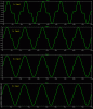
Shown in the first attachment is the result of simulations of a class B amplifier with plus and minus 10 volt power supplies driven with a pure sine source of varying levels starting at 1v peak and doubling up to 8v peak, and a 25k resistor to ground. As clearly shown, the distortion is very bad for lower inputs, but distortion gets lower and lower as the input gets higher and higher. This makes the output stage look better and better. Indeed the harmonics do get lower and lower as the input goes higher, so the output does in fact get cleaner. This is similar to what we might get from the LM358 if we follow the data sheet word for word.
But that's not the end of it of course. The data sheet tells us that to get a crossover free output we need a resistor from the output to *GROUND*. Here's where the confusion comes into play. We all know what ground is, but what the data sheet implies is that GROUND is ground no matter how we hook up the LM358. That isnt true. We already have a resistor to ground and that's the load, and decreasing this value doesnt help much. The mistake is that GROUND on the data sheet actually should read: "The most negative supply voltage", not: "ground" as it does. This leads designers to place a resistor from output to ground, even in dual supply circuits, and it effectively does not help. People using the device more casually notice this too, and they don't like it.
The idea with the output resistor (connected properly that is) is to bias the output stage into class A operation. This means we can get a clean output.
If you look at the second attachment, you'll see the difference. When the amplifier is biased into class A operation we get a much cleaner output even with the lower level input signal because we effectively don't use the lower transistor anymore. The crossover distortion comes from having to wait for one transistor to turn on while the other turns off, but by biasing correctly we never turn anything off, and only use the upper transistor.
The second attachment shows the clean output and that's all because of a single added resistor, but that single added resistor has to be connected properly.
So the output resistor does not always go to ground, it goes to the most negative supply voltage. That may or may not be the true circuit ground. This is something that is absolutely mandatory for correct operation in circuits that need a clean output.
There are still some limitations for the LM358, but now at least we can get a clean output. The limitation for the output to negative rail resistor is probably around 500 ohms, but it depends on power suppply levels so you should test your design. The requirement for this resistor in your application is such that it has to be small enough to be able to pull the load down to the required low level, but not draw so much current that it overloads the output of the LM358. This is often easy to achieve for lower level output requirements. It's only the most demanding output current applications that this may not be possible for. Signal level circuits however should have no problem with this little modification. This should include audio circuits where the output level isnt too high, probably about 3v peak maximum.
Side note:
Ignore the offset voltage in the second attachment. This is because the amplifier used in the simulations did not contain feedback. For a normal LM358 amplifier connection the output would be centered at 0v as usual.
The LM358 gets a bad rap a lot because of various reasons, one of them being the crossover distortion. This is due mostly because the data sheet contains subtle errors about the correct use of the device for many applications that need a clean sine output or just low distortion.
The main crossover problem comes from the output section of the LM358, which is a class B amplifier.
Shown in the first attachment is the result of simulations of a class B amplifier with plus and minus 10 volt power supplies driven with a pure sine source of varying levels starting at 1v peak and doubling up to 8v peak, and a 25k resistor to ground. As clearly shown, the distortion is very bad for lower inputs, but distortion gets lower and lower as the input gets higher and higher. This makes the output stage look better and better. Indeed the harmonics do get lower and lower as the input goes higher, so the output does in fact get cleaner. This is similar to what we might get from the LM358 if we follow the data sheet word for word.
But that's not the end of it of course. The data sheet tells us that to get a crossover free output we need a resistor from the output to *GROUND*. Here's where the confusion comes into play. We all know what ground is, but what the data sheet implies is that GROUND is ground no matter how we hook up the LM358. That isnt true. We already have a resistor to ground and that's the load, and decreasing this value doesnt help much. The mistake is that GROUND on the data sheet actually should read: "The most negative supply voltage", not: "ground" as it does. This leads designers to place a resistor from output to ground, even in dual supply circuits, and it effectively does not help. People using the device more casually notice this too, and they don't like it.
The idea with the output resistor (connected properly that is) is to bias the output stage into class A operation. This means we can get a clean output.
If you look at the second attachment, you'll see the difference. When the amplifier is biased into class A operation we get a much cleaner output even with the lower level input signal because we effectively don't use the lower transistor anymore. The crossover distortion comes from having to wait for one transistor to turn on while the other turns off, but by biasing correctly we never turn anything off, and only use the upper transistor.
The second attachment shows the clean output and that's all because of a single added resistor, but that single added resistor has to be connected properly.
So the output resistor does not always go to ground, it goes to the most negative supply voltage. That may or may not be the true circuit ground. This is something that is absolutely mandatory for correct operation in circuits that need a clean output.
There are still some limitations for the LM358, but now at least we can get a clean output. The limitation for the output to negative rail resistor is probably around 500 ohms, but it depends on power suppply levels so you should test your design. The requirement for this resistor in your application is such that it has to be small enough to be able to pull the load down to the required low level, but not draw so much current that it overloads the output of the LM358. This is often easy to achieve for lower level output requirements. It's only the most demanding output current applications that this may not be possible for. Signal level circuits however should have no problem with this little modification. This should include audio circuits where the output level isnt too high, probably about 3v peak maximum.
Side note:
Ignore the offset voltage in the second attachment. This is because the amplifier used in the simulations did not contain feedback. For a normal LM358 amplifier connection the output would be centered at 0v as usual.
Attachments
Last edited:
")
") And as usual, I will write it all down.
And as usual, I will write it all down.

