GromTag
Active Member
There are cheap supplies available, I just wanted to build my own switching type via simple means, ex, Meanwell USA RS-35-12 for example.... such as cost vs unknown performance via noise. Building my own has shown astounding operational use, tho the primary seperation regulator stage is bothering me with theory vs facts that the facts are not quite clear. I need some sustainment on Facts to weigh in details on an attempt to stop the linear regulators
oscillation on output in this way if it turns out to be an issue not desired by considerate operational means of any design, private use.
If this seems unusual to read, a long all nighter + and continuous thought changes result in sliced and diced Index results.
Subject, general thoughts applied with theory and select listings of Super LDO MIC5156 operation.
I have encountered an issue with a new (new to me) power supply control via an use of an MIC5156 Super LDO regulator controller.
Overly I Am not yet fully familiar with this device even with Google to append information other than what wording to use for an appropriate result to this particular scenario. Am still looking.
:I am unsure why I all ways call this chip Mircel... It's Micrel.
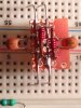
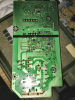
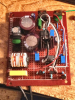
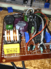
Chip: Micrel MIC5156 Super LDO Adjustable model (Subside of Micro) Details: Low volt supply in 3V, max high 38V, 36V listed as preferred limiting supply. I am not approaching max voltage if I can maintain form of any supply have / use.
I am a bit perplexed of what I have caused in an experiment acquiring to divert the primary used supply into dual LDO banks to provide limited power to the VP pin 4 MOSFET gate drive power supply, those results latter on.
1 main supply, 2 linear regulators, 1 per VP pin, 2 switching LDO banks supplying 5V to 2 different sub arrays, CMOS, gates, Comparators, OpAmps. Comparators fast saturated switchers, direct drivers to gate logic, OpAmps, Unity buffer for
long line return from source being driven by unity op amps without the use of differential pair of needing negative voltage requirement. Avg 25 Ft length 24 gauge stranded Harbour Freight shielded wire.
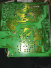
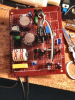
As of, I only have the L4940 with the internals in design to use and is fixed at 5V that stays cool under operation. That was the initial start testing thought, have been proven wrong. Details below. (quick ref, the regulators output is greater than the stated out with adequate grounding and respect to distance from LDO). layout = power in, L4940 - LDO - FET power out.
FET Details, MOSFET model: ST STP100N8F6.
I'm using a linear regulator to produce 5V fixed, model: ST L4940 to produce 5V with sustaining capacitors for bulk low and capacitors for high frequency ends to allow an reasonable amount of power to LDO pin 4 VP Fet supply drive to power the FET switch push pull driver in direct link with LDO Gate drive pin 6 to the FETs Gate negating the length of wire avg 1 inch at 20 gauge multi strand high voltage pre soldered. Thus far no direction formed towards any pull down resistor to assist Gate drive shut down and removal of potential excess of transient voltage surge, that is not yet being covered, however an 16V zener model: Vishay Semiconductor IN5246B-TR @ 500mW DO35 mounting type is used to allow pass of in case excess voltage to the FET gate that is rated at the avg of 20V. :Frequency reaction loss of potential Zener reaction for FET gate
overvoltage is an known acceptance of loss if occurs:
The FET gate is at this point at its low drive voltage. Or it should be, thus far the power to the FET has not dropped below 8V. Explanations below "Issue".
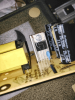
Power supply #1 details:
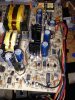
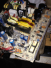
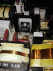
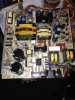
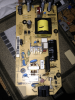
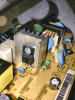
The initial supply is dual switching 120V to 240V A/C input with 12V out that when not loaded can assume at 16V level, no problems other than this supply is very noisy for an switching supply. The supply does manage the power required and current, It is an salvage board with unknown current rating, however the rating should easily supply at least up to near 2.5 amps via the secondary fuse used on board against the primary fuse of 3.15 amps as the delay glass fuse.
(I did not like this supplies noise, discontinued its use)
Power supply #2 details:
120V A/C only, output 20V stable, an ideal switching supply on non existent noise, currently used thus far and may continue to use.
The supply is an salvaged (repurposed) Direct TV out door unit, satellite SWM ODU SWiM line driver with the line drive inductor removed and the lines applied for direct connect power use. Current varies under heavy use, stable to 1Amp.
No noticeable noise to 250mA draw.
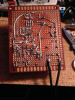
Issue : The L4940 5V fixed regulator on the 12V supply displayed at avg 9.3V on its output with no heat produced, the LDO was being applied 12.3V on the VDD pin 5, the fet was getting near exact rating of 9.3V from the LDO VP component with no fluctuation and the LDO, EA ADJ from FET Source output was trimmed to 5V on the nose, The FET Source output was stable to an T at 5V, held fine to the thus far tested limit of 100R @ 50mA with only 1.4 mV avg drop on the FET Source output (some minor grounding issues still for line of current sight for the MIC5156 supply driver) Capacitor stages used to result in stable non jitter FET Source output as to the (Victor 70C.) level rating not showing
oscillating result.
:issue : So the problem, the driving stage of the LDO VP is likely feeding back to the L4940 regulator resulting in a current pull supply overdrive like response from the fixed regulators P channel BJT in term supplying the LDO to FET gate with
near the rated power from the regulators output greater than the fixed stated value of 5V regulator avg resulting in an output of 9.3V from the regulator itself. (charge pump effect)
My concern is if this is like an inductive response between the regulator and the LDO switching causing a voltage rise as this be problematic such as reliance of sustained use? Wording of sorts lacking as I do not know of appropriate
wording of the scenario.
:Next, power supply #2:
Power supply #2 @20V stable even with no load.
Same issue with L4940 5V regulator except the out put from regulator this supply is 18.3V, I am going no further on voltage as 1, no other supply of higher voltage is avail to me and 2, I an applying more possible pressure to the unknown scenario resulting. Thus the output is again even more stable with the low noise supply #2 and shows only 1/2 mV loss on FET Source out with the 100R when applied.
Issue : Again what is the problem? Well focusing on the L4940 schematic it uses a P channel BJT to drive the output with protection and an error amplifier, my thoughts are that is an induction effect is occurring between the regulator and LDO that I am causing the error amp to step in and the side results of a P channel BJT that can allow for a higher voltage on collector out before device reaction along with the thoughts on the LDO FET push pull stage design being
somewhat thought out by design to expect some oscillation on the VP pin 4 supply that in the event is plausible for sustained operation in this configuration. Other thoughts are that the oscillation is too great for safe device operation of either the regulator or the LDO and both in between. Append question as, this can not be good for the device states my most thoughts for continued operation as such?
Main concept theory, a potential poor make shift inductor charge boost applied on the LDO VP input resulting in an charge pump effect to the FET gate is what could be occurring. It looks it.
Thus far running at 20V supply #2 for a day straight has yielded no problematic results even on an solderless board. Thou I have a thought if I load too much draw from the FET that could change the distinction between the regulator and the LDO causing a list of potential problems to occur.
The power supply #1 is avg at 150kHZ. supply #2 I can not gauge, Zeroes. Even through the regulator onto the FET and on down stream I can not gauge the power supply #2 switching frequency.
Other regulators such as the KA7809 for 9V fixed resulted in fast pace overheat on the 20V supply, the most reason for this is the internals contain a current generator with a starting circuit, technical switching linear regulator.
The same with KEK KIA7805 and others alike the 7805, the oscillation is causing the issue with those types yet not burdening the P channel linear types with extreme heat build up at ither #1 or #2 power supply used.
I may not need to split the supply to the LDO in any way. Why producing two power methods? 1 is filtered for uA current logic CMOS gate and drivers with the thoughts on power filtering and sustained, and the other drive affected by FET driver stage noise to append power to the main array of current hungry phototriacs with an avg of 10-15 mA each, 5 used thus far. No exponent room of current consumption chosen yet for added head room from switching supply.
Power stages split from main supply to not affect trimmed adjustment voltage via current draw from other devices.
Most documentation encountered states of the difference of the LDO vs linear regulator in difference, not about using an linear regulator to drop power to any input.
Linear AN140-4 states some close points of the linear pass element resulting in inefficient power output via percentage thou not seeing any thing alike the above mentioned.
A few regulators used / listed in PDF form including MIC5156 and FET STP100N8F6, the L4940 is currently in use now with supply #2, no noticeable temperature issue with power supply #2 @ 20V, with 18.3V on the regulators output with overall low current use, main current check for idle is not capable, need a 500mA glass fuse for tool, brushed a power pin when sereis when checking aa adjacent drive current. The gate drive from the LDO to FET gate is currently 8.56V, the 12V supply #1 was 9.3V gate drive from LDO, L4940 reg.
L7805CV regulator was an oversized file, omitted.
oscillation on output in this way if it turns out to be an issue not desired by considerate operational means of any design, private use.
If this seems unusual to read, a long all nighter + and continuous thought changes result in sliced and diced Index results.
Subject, general thoughts applied with theory and select listings of Super LDO MIC5156 operation.
I have encountered an issue with a new (new to me) power supply control via an use of an MIC5156 Super LDO regulator controller.
Overly I Am not yet fully familiar with this device even with Google to append information other than what wording to use for an appropriate result to this particular scenario. Am still looking.
:I am unsure why I all ways call this chip Mircel... It's Micrel.
Chip: Micrel MIC5156 Super LDO Adjustable model (Subside of Micro) Details: Low volt supply in 3V, max high 38V, 36V listed as preferred limiting supply. I am not approaching max voltage if I can maintain form of any supply have / use.
I am a bit perplexed of what I have caused in an experiment acquiring to divert the primary used supply into dual LDO banks to provide limited power to the VP pin 4 MOSFET gate drive power supply, those results latter on.
1 main supply, 2 linear regulators, 1 per VP pin, 2 switching LDO banks supplying 5V to 2 different sub arrays, CMOS, gates, Comparators, OpAmps. Comparators fast saturated switchers, direct drivers to gate logic, OpAmps, Unity buffer for
long line return from source being driven by unity op amps without the use of differential pair of needing negative voltage requirement. Avg 25 Ft length 24 gauge stranded Harbour Freight shielded wire.
As of, I only have the L4940 with the internals in design to use and is fixed at 5V that stays cool under operation. That was the initial start testing thought, have been proven wrong. Details below. (quick ref, the regulators output is greater than the stated out with adequate grounding and respect to distance from LDO). layout = power in, L4940 - LDO - FET power out.
FET Details, MOSFET model: ST STP100N8F6.
I'm using a linear regulator to produce 5V fixed, model: ST L4940 to produce 5V with sustaining capacitors for bulk low and capacitors for high frequency ends to allow an reasonable amount of power to LDO pin 4 VP Fet supply drive to power the FET switch push pull driver in direct link with LDO Gate drive pin 6 to the FETs Gate negating the length of wire avg 1 inch at 20 gauge multi strand high voltage pre soldered. Thus far no direction formed towards any pull down resistor to assist Gate drive shut down and removal of potential excess of transient voltage surge, that is not yet being covered, however an 16V zener model: Vishay Semiconductor IN5246B-TR @ 500mW DO35 mounting type is used to allow pass of in case excess voltage to the FET gate that is rated at the avg of 20V. :Frequency reaction loss of potential Zener reaction for FET gate
overvoltage is an known acceptance of loss if occurs:
The FET gate is at this point at its low drive voltage. Or it should be, thus far the power to the FET has not dropped below 8V. Explanations below "Issue".
Power supply #1 details:
The initial supply is dual switching 120V to 240V A/C input with 12V out that when not loaded can assume at 16V level, no problems other than this supply is very noisy for an switching supply. The supply does manage the power required and current, It is an salvage board with unknown current rating, however the rating should easily supply at least up to near 2.5 amps via the secondary fuse used on board against the primary fuse of 3.15 amps as the delay glass fuse.
(I did not like this supplies noise, discontinued its use)
Power supply #2 details:
120V A/C only, output 20V stable, an ideal switching supply on non existent noise, currently used thus far and may continue to use.
The supply is an salvaged (repurposed) Direct TV out door unit, satellite SWM ODU SWiM line driver with the line drive inductor removed and the lines applied for direct connect power use. Current varies under heavy use, stable to 1Amp.
No noticeable noise to 250mA draw.
Issue : The L4940 5V fixed regulator on the 12V supply displayed at avg 9.3V on its output with no heat produced, the LDO was being applied 12.3V on the VDD pin 5, the fet was getting near exact rating of 9.3V from the LDO VP component with no fluctuation and the LDO, EA ADJ from FET Source output was trimmed to 5V on the nose, The FET Source output was stable to an T at 5V, held fine to the thus far tested limit of 100R @ 50mA with only 1.4 mV avg drop on the FET Source output (some minor grounding issues still for line of current sight for the MIC5156 supply driver) Capacitor stages used to result in stable non jitter FET Source output as to the (Victor 70C.) level rating not showing
oscillating result.
:issue : So the problem, the driving stage of the LDO VP is likely feeding back to the L4940 regulator resulting in a current pull supply overdrive like response from the fixed regulators P channel BJT in term supplying the LDO to FET gate with
near the rated power from the regulators output greater than the fixed stated value of 5V regulator avg resulting in an output of 9.3V from the regulator itself. (charge pump effect)
My concern is if this is like an inductive response between the regulator and the LDO switching causing a voltage rise as this be problematic such as reliance of sustained use? Wording of sorts lacking as I do not know of appropriate
wording of the scenario.
:Next, power supply #2:
Power supply #2 @20V stable even with no load.
Same issue with L4940 5V regulator except the out put from regulator this supply is 18.3V, I am going no further on voltage as 1, no other supply of higher voltage is avail to me and 2, I an applying more possible pressure to the unknown scenario resulting. Thus the output is again even more stable with the low noise supply #2 and shows only 1/2 mV loss on FET Source out with the 100R when applied.
Issue : Again what is the problem? Well focusing on the L4940 schematic it uses a P channel BJT to drive the output with protection and an error amplifier, my thoughts are that is an induction effect is occurring between the regulator and LDO that I am causing the error amp to step in and the side results of a P channel BJT that can allow for a higher voltage on collector out before device reaction along with the thoughts on the LDO FET push pull stage design being
somewhat thought out by design to expect some oscillation on the VP pin 4 supply that in the event is plausible for sustained operation in this configuration. Other thoughts are that the oscillation is too great for safe device operation of either the regulator or the LDO and both in between. Append question as, this can not be good for the device states my most thoughts for continued operation as such?
Main concept theory, a potential poor make shift inductor charge boost applied on the LDO VP input resulting in an charge pump effect to the FET gate is what could be occurring. It looks it.
Thus far running at 20V supply #2 for a day straight has yielded no problematic results even on an solderless board. Thou I have a thought if I load too much draw from the FET that could change the distinction between the regulator and the LDO causing a list of potential problems to occur.
The power supply #1 is avg at 150kHZ. supply #2 I can not gauge, Zeroes. Even through the regulator onto the FET and on down stream I can not gauge the power supply #2 switching frequency.
Other regulators such as the KA7809 for 9V fixed resulted in fast pace overheat on the 20V supply, the most reason for this is the internals contain a current generator with a starting circuit, technical switching linear regulator.
The same with KEK KIA7805 and others alike the 7805, the oscillation is causing the issue with those types yet not burdening the P channel linear types with extreme heat build up at ither #1 or #2 power supply used.
I may not need to split the supply to the LDO in any way. Why producing two power methods? 1 is filtered for uA current logic CMOS gate and drivers with the thoughts on power filtering and sustained, and the other drive affected by FET driver stage noise to append power to the main array of current hungry phototriacs with an avg of 10-15 mA each, 5 used thus far. No exponent room of current consumption chosen yet for added head room from switching supply.
Power stages split from main supply to not affect trimmed adjustment voltage via current draw from other devices.
Most documentation encountered states of the difference of the LDO vs linear regulator in difference, not about using an linear regulator to drop power to any input.
Linear AN140-4 states some close points of the linear pass element resulting in inefficient power output via percentage thou not seeing any thing alike the above mentioned.
A few regulators used / listed in PDF form including MIC5156 and FET STP100N8F6, the L4940 is currently in use now with supply #2, no noticeable temperature issue with power supply #2 @ 20V, with 18.3V on the regulators output with overall low current use, main current check for idle is not capable, need a 500mA glass fuse for tool, brushed a power pin when sereis when checking aa adjacent drive current. The gate drive from the LDO to FET gate is currently 8.56V, the 12V supply #1 was 9.3V gate drive from LDO, L4940 reg.
L7805CV regulator was an oversized file, omitted.
Attachments
Last edited:

")