electrookie
New Member
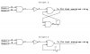
Hi all;
In the attached drawing, I am trying to figure if I got it right or not. What I am after is a Logic circuit that will latch upon a certain condition and will not toggle till a reset switch is depressed. I have been searching the web and have pieced together this circuit. I am going to build it next, but thought I would run it up the flag pole for some comments.
The goal is when the 2 inputs (labeled outputs) are high, the flip flop will turn the Q on and the Q' off, the Q will be sent to a relay to turn it on. The 10uf cap and 1M resis on the reset line are to insure power on condition of Q off and Q' on.
If this looks like I got it right, then please do let me know. However, as I suspect, I probably have something wrong here, then your input will be invaluable. I will go build this now and check back later to see if anyone replied and to post my results.
Thanks all in this forum...
OOOPPP's... The AND gates shown are supposed to be NAND gates, so keep this in mind when examining circuit. Thanks again...
Attachments
Last edited: