Continue to Site

Welcome to our site!

Electro Tech is an online community (with over 170,000 members) who enjoy talking about and building electronic circuits, projects and gadgets. To participate you need to register. Registration is free. Click here to register now.

  • Welcome to our site! Electro Tech is an online community (with over 170,000 members) who enjoy talking about and building electronic circuits, projects and gadgets. To participate you need to register. Registration is free. Click here to register now.

Isolated driver reverse protection query/simulation

Status
Not open for further replies.

ACharnley

Member
Hi,

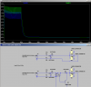
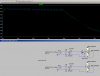
Just hoping for another set of eyes to ensure I've got this right. Here's an isolated fet driver circuit with fast discharge.

Screenshot_2019-12-19_13-10-17.png


I thought R11 with C3 would act as a filter but the value isn't having much an effect. My understanding is C3 allows the PWM to pass, too small a value and the PWM frequency won't get through (so C3 is the main part of the filter).

The driver switches low frequency, low voltage AC but the AC is rectified someplace else and ends up providing the PWM, therefore there's a loop and potentially high frequency noise and the alike could follow the red arrow back to the voltage source (and blow it), therefore the voltage source requires a TVS and a higher value of C3 works to restrict said noise from making it back in the first place.

PWM frequency is at least 1MHz to keep the FET on using it's internal gate capacitance.

While I'm at it, the fast gate discharge I nicked from another circuit and while it simulates as working I'm curious as to how. Being a PNP I expected the gate had to be pulled down to ground to discharge whereas when the PWM stops both the voltage at gate/emitter is at the same value, other than a *very* minor voltage drop by way of the diode reverse current and R13?
 
u1,u3: pin2=Gate? pin1=Source? or maybe Drain?

"Fast turn off" is not working. There is nothing to turn on Q4.
 
Last edited:
That transistor circuit needs a drive signal that is active for both high and low levels.

The high to turn on the FET and the low to pull current through the transistor base-emitter junction so it turns on and pulls the FET gate low.
It would also need a low value series resistor, so base current has some limiting.
 
I did think it was odd which is why I mentioned it.

I found this in the VOM1271 datasheet. I guess the guy in the link above meant P-JFET not PNP.

Screenshot_2019-12-19_19-58-20.png


I have simulated the above with various JFET's in LTSpice and it doesn't work at all.
 
Last edited:
Added a diode D1 to make turn on faster. Added C2.
Increased drive voltage from 5 to 10. 3 volts is not enough to turn on a MOSFET.
Added R3 for turn off.
Green trace is Gate to Source voltage.
Are you trying to make a solid state realy?
1576788313304.png
 
Yes, attempting to avoid VOM1271 due to the high cost and footprint size (I need several of them per PCB).

Your addition is worse than a resistor. ;)

Screenshot_2019-12-19_21-06-19.png
 
I don't have those FETs so I've just substituted a cap for the gate load.

Using the same 33K discharge resistor in each case (rather than different values), Ron's modified version with the diode seems to give a vastly improved discharge, using your original sim with the modifications.
That's with either 5V or 10V drive.

Green = rectifier output, blue = upper version "gate" cap, red = lower version gate cap.

I'd guess the rec output cap needs to be sized in proportion to the gate capacitance, to keep the ripple reasonable without unduly slowing the turn-off stage??

fetdriver.jpg
 

Attachments

  • fetdrive-isolate-pwm-compare.asc
    3.6 KB · Views: 171
I must be blind then, I'm basically after VOM1271 at a more reasonable price point. I estimate this capacitor based drive circuit will cost 10c each vs 75c+ of a VOM1271, and each circuit has several. Toshiba do a similar one as well but same price point.

I've ran spice on the main circuit and using the FET's I've chosen a 33k isn't fast enough. The issue with going down to 10k is the ripple at 5v PWM is pulling the FET into low Vgs territory which will make heat. (these FET's ideally need a 4.5v drive).

Using your idea I can make the equivalent of a 3.3k but I'll have to add a boost and a driver for each circuit (I was driving directly from 5V PIC). Not a dealbreaker and still a big saving over multiple VOM1271.
 

Attachments

  • Screenshot_2019-12-20_16-48-47.png
    Screenshot_2019-12-20_16-48-47.png
    33.5 KB · Views: 201
Would you say R1 is necessary? It reduces efficiency of the drive but was originally inserted to limit backflow noise/spikes on the AC line (which shouldn't happen..). I was originally using 0.1u but switched to 22n for higher frequency and in doing so I wonder if the 22n alone will be enough to prevent backflow.
 
How much isolation do you need.
Is the load AC or DC or both?
Do you have a higher voltage available? 12V??
I often use a pulse transformer for isolation and gate drive. If the VOM1271 brakes the bank a transformer is about the same price.
 
100V peak, switching in capacitance into an inductive AC line (hence transients).

I'll use a boost to get 12V they're only $.05c from China, no problem there. Transformer impossible, so is the SO-8 the VOM1271 uses (I forgot about that). Max component height is 1.2mm.

Anyhow I'm happy with the performance/price/combined footprint size of the FET discharge as it is.
 
Have you looked at surface mount mini relays? About 1/2 the price for a solid state relay.

Many water timers use opto-triac for switching 24V ac.
----edited-----
I thought I could find a 2A opto triac but no.....
1576867882600.png
 
Last edited:
I've been battling the turn-off but haven't nailed it yet. Initially I thought the turn-off issue was about draining the gate, but switching to VOM1271 for a comparison yields the same result.

The green is the PWM signal off / VOM LED power off. You can see the floating voltage component reduce at the start. It's quite a bit slower with the 1271 than the capacitor based drive circuit in the previous posts. At this point I'd expect the current going through to fall to zero but you can see (blue) the fall is gradual over .5ms.

Screenshot_2019-12-20_23-13-00.png
 
Status
Not open for further replies.

Latest threads

New Articles From Microcontroller Tips

Back
Top