Continue to Site

Welcome to our site!

Electro Tech is an online community (with over 170,000 members) who enjoy talking about and building electronic circuits, projects and gadgets. To participate you need to register. Registration is free. Click here to register now.

  • Welcome to our site! Electro Tech is an online community (with over 170,000 members) who enjoy talking about and building electronic circuits, projects and gadgets. To participate you need to register. Registration is free. Click here to register now.

Inverting a modulated signal (OOK).

Status
Not open for further replies.

Alex_bam

New Member
Hello,
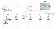
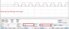
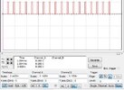
I'm modulating the message signal with OOK (on-off keying) modulation. Multisim software is used to model the schematic [attached]. At the resistor R1, the modulated signal is obtained. I wanted to invert the modulated single, for that I used a simple NOT gate (U3), however at the NOT's gate output, I got the same signal as input means without inverting [attached]. So my question is, why isn't the NOT gate inverting? Am I doing something wrong?

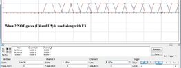
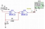
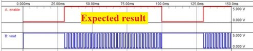
As hit and trail, I added two more NOT gates (U4 and U5) but this time I got an inverted signal, although further improvement is needed to achieve a 180-degree phase shift. So my second question is: Why is it an inverter this time? and how to get exactly a 180-degree phase shift between two signals?

Thanks for your time.
 

Attachments

  • 3.JPG
    3.JPG
    97.9 KB · Views: 192
  • 1.JPG
    1.JPG
    114.1 KB · Views: 188
  • 2.JPG
    2.JPG
    101.1 KB · Views: 179
You don't give a part number for the NAND gate, so we don't know if it has hysteretic inputs. And, usually there is a resistor in the feedback path for more control and stability of the oscillating frequency.

Beyond all of that, the oscillator probably is producing a symmetrical output, which looks the same on a scope inverted or not because of how a scope trigger works. The extra inverters are merely a delay line, giving a time-shifted (not inverted) image.

What is the purpose of R1?

ak
AnalogKid Thanks for your response. Based on your suggestion, I tried another schematic [attached], in which the resistor is used as feedback, I have mentioned the source from where I got this schematic, however, this schematic also did not work although I followed all the design steps for calculating the R and C.

The formula for calculating oscillating freq (Fc), R and C: Fc=1/2.2RC

Could you please review it? where I am making mistake?

Link: https://www.allaboutcircuits.com/technical-articles/how-to-design-schmitt-trigger-oscillators/
 

Attachments

  • 4.JPG
    4.JPG
    88.6 KB · Views: 176
  • 5.JPG
    5.JPG
    51.9 KB · Views: 182
  • 6.JPG
    6.JPG
    39 KB · Views: 178
Status
Not open for further replies.

Latest threads

New Articles From Microcontroller Tips

Back
Top