ThermalRunaway
New Member
Hi everyone,
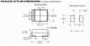
I've been busy on my latest project, and I'm doing my own PCB design. Naturally, most of the parts I need aren't in the Eagle library so I'm creating my own footprints. So far I've been okay (apart from the regular annoyance of inferred dimensions - just bloody state them all!). But I've just come across a package outline document for a schottky diode, which I thought would be easy-peasy, but I'm really confused by it.
Please see the image attached.
What I want to know is, why are there two sets of numbers for the dimensions on this diagram? For example, the body width has a figure of 6.22mm and a figure of 5.59mm underneath. So... which one is it? I've tried both and actually neither of them look quite right.
Am I missing something obvious here?
Thanks in advance for the advice,
Brian
Attachments
Last edited:
