Explain!! Do you mean the commands work but not the data?... If so how do you know??
The code you posted will not show anything even if the LCD somehow boots to 8 bit...
There is another command in the set up that turns the display on/off , writing 0xC0 will turn it on..
Both command and data work.The only (or so far only) bug is that it would not go to the second line (0xC0) and there are one unwanted space between the characters.
See this film!(sorry film didn,t upload)
and this is the code:
void main()
{
DDRA=0xff; // making LCD_DATA port as output port
DDRB=0xff; // making signal as out put
DDRC=0xff;
PORTB=0xff;
PORTB.4=0; //buzer
delay_ms(200);
PORTB.4=1;
PORTB.0=0; //v0 lcd
PORTA.1=0;//w
PORTA.7=0;//enable 595
HC595Init();
delay_ms(10);
init_LCD(); // initialization of LCD
delay_ms(100); // delay of 50 milli seconds
while(1)
{
lcd_gotoxy(2,0);//this dose not work
LCD_write('A');
LCD_write('B');
LCD_write('C');
LCD_write('D');
LCD_write('E');
// LCD_cmd(0x18);
LCD_write('F');
LCD_write('G');
LCD_write('H');
LCD_write('I');
LCD_write('J');
LCD_write('K');
LCD_write('L');
LCD_write('M');
// LCD_cmd(0x18);
LCD_write('N');
delay_ms(2000);
LCD_cmd(0x01);
LCD_cmd(0xc0);//this dose not work
LCD_write('O');
LCD_write('P');
LCD_write('Q');
LCD_write('R');
LCD_write('S');
LCD_write('T');
LCD_write('U');
// LCD_cmd(0x18);
LCD_write('V');
LCD_write('W');
LCD_write('X');
LCD_write('Y');
LCD_write('Z');
LCD_write(' ');
delay_ms(2000);
LCD_cmd(0x01); //clear the screen
delay_ms(1000);
}
}
void init_LCD(void)
{
LCD_cmd(0x38); // initialization of 16X2 LCD in 8bit mode
delay_ms(1);
LCD_cmd(0x01); // clear LCD
delay_ms(1);
LCD_cmd(0x0E); // cursor ON
delay_ms(1);
//LCD_cmd(0x80); // ---8 go to first line and --0 is for 0th position
//delay_ms(10);
return;
}
void LCD_cmd(unsigned char cmd)
{
LCD_DATA=cmd;
HC595Write(cmd);
rs=0;rw=0;en=1;//ctrl =(0<<rs)|(0<<rw)|(1<<en); // RS and RW as LOW and EN as HIGH
delay_ms(1);
rs=0;rw=0;en=0;//ctrl =(0<<rs)|(0<<rw)|(0<<en); // RS, RW , LOW and EN as LOW
delay_ms(5);
return;
}
void LCD_write(unsigned char data)
{
LCD_DATA= data;
HC595Write(data);
rs=1;rw=0;en=1;//ctrl = (1<<rs)|(0<<rw)|(1<<en); // RW as LOW and RS, EN as HIGH
delay_ms(1);
rs=1;rw=0;en=0;//ctrl = (1<<rs)|(0<<rw)|(0<<en); // EN and RW as LOW and RS HIGH
delay_ms(5); // delay to get things executed
return ;
}

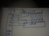
 in 13 is the enable of 595 which must be zero to be selected .pin 39 is also zero in this case all the time.