Continue to Site

Welcome to our site!

Electro Tech is an online community (with over 170,000 members) who enjoy talking about and building electronic circuits, projects and gadgets. To participate you need to register. Registration is free. Click here to register now.

  • Welcome to our site! Electro Tech is an online community (with over 170,000 members) who enjoy talking about and building electronic circuits, projects and gadgets. To participate you need to register. Registration is free. Click here to register now.

Improving storage time

Status
Not open for further replies.

MacIntoshCZ

Active Member
Hello,
i know some techniques to improve storage time, but not all can be always used.
I would like to see whats inside 10A mosfet driver cause i spend to much time solving this problem.
Those i know so far. I do not want to use 10A mosfet driver until i am able to make one myself.
R12 is sometimes a problem. When i have some aplification cause pwm is delivering 10mA, first step is 100mA, then 1A and finnal 10A.
R12 some times need to be low value, but when its too loow it bypassing driving signal... Those schematics are just example. Real schematic is lost (energy distributor failere -> pc turned off, thank you energy distributor =)...), so this would be a shitty question.
Is there any other option to fast turn off transistor from saturation in power electronics?
I am not facing slow turn on, just turn off is problem. I know that instead of 1n4148 schottky should be used.
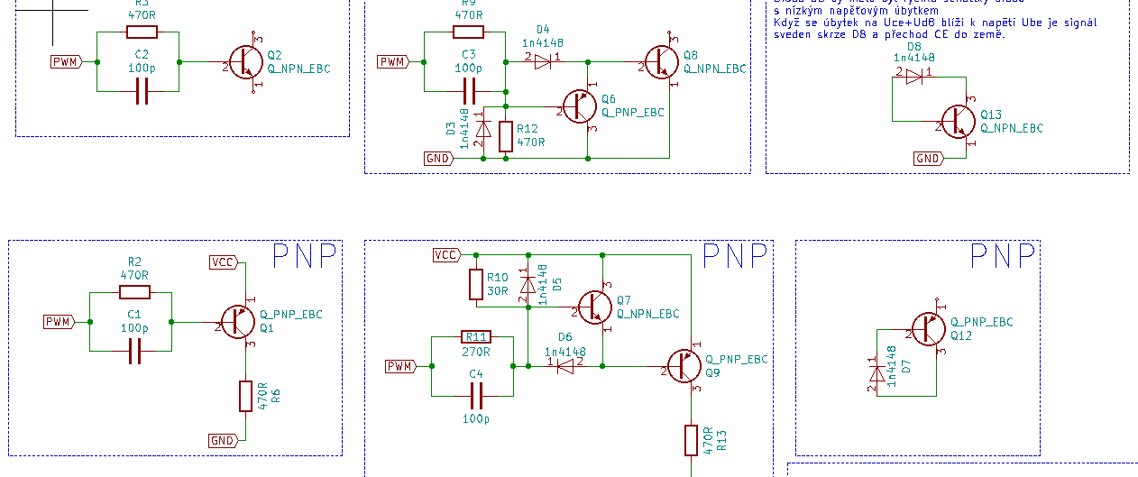
1608737431908.png
 
Last edited:
i know some techniques to improve storage time
Are you talking about large bipolar transistors? (not MOSFETs) High voltage transistors have very large storage delay times.

Data sheets on HV HC power transistors often have graphs showing storage time verses gain, collector current and IB2 current.
>If you drive the transistor hard on, large Base current with very low Vce the delay will be very long. Starving the Base until the Collector voltage just starts up will reduce the delay.
>Baker clamp: Some of the Base current will flow through D1 and then C-E-ground. This keeps the transistor in the linear region and out of the hard on area. Base current is limited to what just keeps the transistor on and not any more. This is a good circuit that works over a wide range of Bata or Hfe if the transistors. You can play games with different types of D1/D2 to get the turn on voltage just right.
1608743180528.png

>Large HV transistors might take 5A of IB1 turn on current. For the storage delay time I would pull down with 15 to 20A to get the part turned off. (usually IB2, the turn off current will approach the IC) I do not pull down to 0V but pull from -5 to -12V. (depends on what type of transistor and what the negative B-E break down voltage is)

I do not know what type of transistors you are using. Don't over drive. Maybe use Baker Clamp. Pull current back out of the Base (hard) during Delay time.
IB1 is Base turn on current, IB2 is pulling the energy back out of the Base. (IB2 current has nothing to do with capacitance) During storage delay time the base is positive even though we are pulling down hard. (IB2 charge is more like a battery and not like a capacitor)
1608743873150.png
 
I was talking about "average" transistors, small ones. Like SS8050.
Whats usage of D2 in baker clamp? Its just additional voltage drop ?
I think i cant use resistor for Ib2 due driving signal losses.
 
Whats usage of D2 in baker clamp?
Q1 E=0V, Q1 B=0.65V, (node Rb,D1, D2)=1.3V, Vin= 3 to 5V,
When Q1 is off and Collector voltage is high, All of I2 goes into the Base to turn on the transistor.
When Q1 is on excess Base current goes through D1 and off to ground via Q1.
Assuming D1 is the same type as D2 (do not have to be the same).
As soon as Q1-C drops below 0.65V, D1 steels off Base current.
1608753413799.png

Redrew circuit so you can see where the current goes. In production some transistors need more or less current and this circuit adjusts for that.
1608754108003.png
 
In my schematic i used only D1. Yours schematic with two diodes seems logical to me. Without D2 IT should steel current near zero voltage on Q1c. Forward voltage drop on diode should be lower than drop on Qbe. Am i right?
 
Yes, you can also use a Schottky diode for one or use a 1n4001 and a 1n4007 (low & high voltage) to get different voltages.
Hello, i tried to do same for pnp in more complex schematic but i think in this case it cant be implemented for Q2, cause it only bypass current for Q1
But when i deleted it it makes oscillation worse... So i dont know =)
1608975411395.png
 

Attachments

  • Draft9.asc
    4.4 KB · Views: 169
Last edited:
Q3 is never on hard so the storage delay there is nothing.
Increased the current in R2 and R9//R11 to 60+mA where the transistor runs faster.
L1 could be removed. I just can not get more than 1.5A in Q5.
1609038314479.png
 

Attachments

  • Draft9-ron.asc
    4.3 KB · Views: 176
Playing about a bit with this, the problem seems to be just insufficient base drive current to the transistors feeding the FET gate.

After numerous variations, a simple brute-force method seems to give the best results...

GateDrive_RJ.png
 

Attachments

  • GateDrive_RJ.asc
    4.1 KB · Views: 168
I realised that had a darlington double junction drop; changing to complementary Sziklai style config improves it a bit more.


GateDrive_RJ_2.png
 

Attachments

  • GateDrive_RJ_2.asc
    4.3 KB · Views: 157
Status
Not open for further replies.

Latest threads

New Articles From Microcontroller Tips

Back
Top