Continue to Site

Welcome to our site!

Electro Tech is an online community (with over 170,000 members) who enjoy talking about and building electronic circuits, projects and gadgets. To participate you need to register. Registration is free. Click here to register now.

  • Welcome to our site! Electro Tech is an online community (with over 170,000 members) who enjoy talking about and building electronic circuits, projects and gadgets. To participate you need to register. Registration is free. Click here to register now.

IGBT-inverter driver ...for Ac motor--need help!!

Status
Not open for further replies.

mananshah93

New Member
I am trying to make ac motor driver on the concept of IGBT-inverter, but I can't able to get desired result...

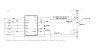
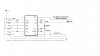
first of all see the attached circuit ...

Q1,Q2,Q3 AND Q4 are 4 N-channel IGBTs -7N60B....they are connected in pair as shown in figure..
I am turning on the Q1 and Q4 by giving 5V to the gate and turning off Q2 and Q3 by giving 0V to their gate...
Now my Vdd=12V...so in this condition I should get 12 V at V1 point , but I am just getting 1.6-2V at that point...V2 is alright at 0V as it should be but V1 is not....

my all 4 igbts are working correct when I test them individualy as a switch, but when I connect like this I do not get the resultss...

Any thing wrong in the circuit??
please reply..
 

Attachments

  • IGBT-CIRCUIT.jpg
    IGBT-CIRCUIT.jpg
    24.5 KB · Views: 7,193
The voltage to the base of the high-side IGBTs must be 5v HIGHER than it's emitter. But because it's high side, some of the base voltage is getting dropped while going through the load to ground.

Try measuring the voltage from base to emitter on the high side IGBTs and you'll see they are not at 5v. You need a bootstrap capacitor and diode to make this happen. There is another thread that has a good diagram of this, but I can't find it at the moment.
 
Last edited:
The voltage to the base of the high-side IGBTs must be 5v HIGHER than it's emitter. But because it's high side, some of the base voltage is getting dropped while going through the load to ground.

Try measuring the voltage from base to emitter on the high side IGBTs and you'll see they are not at 5v. You need a bootstrap capacitor and diode to make this happen. There is another thread that has a good diagram of this, but I can't find it at the moment.

thanx, I will try this, now want to make sure...if I am not wrong , electrolyte capacitor is used and positive should be connected to source(V=12v in my circuit or to the gate?) and negative to the emitter...

I am also confused about which value of capacitor to take?
 
These are IC's designed specifically for what you need. I use them all of the time and with great results.
 

Attachments

  • IR2110 - IR2113 HALF BRIDGE DRIVER.pdf
    210.3 KB · Views: 1,963
Page 4 has the specific IC pin layouts. The first page schematic is basically what I use. Just make sure the SD pin is connected to the common line and not left floating if its not being used.

The blank pins can be trimmed off of the IC without problems though.
 
Page 4 has the specific IC pin layouts. The first page schematic is basically what I use. Just make sure the SD pin is connected to the common line and not left floating if its not being used.

The blank pins can be trimmed off of the IC without problems though.

Thanx again....still I have some doubts regarding VDD, VS and VB....I am not clear about these 3...
what I understand is If SD is low and VCC is supplied then what will be the input to HIN and LIN, that will be passed to HO and LO...
am I right??

What is logic supply>VDD
I have to connect emitter of upper IGBT to pin Vs???
can u help out?
 
For the VCC and VDD voltage I typically use a 15 volt source. Most IGBT'S have 20 - 25 volt gate voltage limits and minimum saturation voltages of 10 volts or so.

The actual logic input Hin, Lin work with any 3.3 volt or higher input up to the VCC and VDD voltage used.

VSS is your common ground point.
As long as your logic system and the supply power to the IC use a common ground reference you wont have any problems.

VB is the voltage source that drives the high side IGBT. The capacitor between VB and VS holds the charge needed to keep the gate voltage above the emitter voltage during the on cycle. That is actually where the floating voltage source comes from.

Depending upon the gate capacitance of the IGBT and the operating frequency or duration of the on time that capacitor may be anywhere from .1 uf to possibly 100uf.
Big gate capacitances and long duration on times will take large capacitors but small gate capacitances with high switching frequencies only need little capacitors.

The .1uf and 10 uf in parallel shown on the one schematic in the spec sheet is typically what I use.
 
I am not able to get the results with ir2110, I am explaining what I have done.

case 1: I have used 2 igbts connected in a pair/half bridge...I have put a 100 ohm resistance between high side emitter and low side collector...
In IR2110, Vcc=Vdd=15 V, used 0.1uF and 1uF connected in parallel as shown in datasheet..Vb is supplied through 1N4007 diode from Vcc..
10uF capacitor between Vb and Vs...

look in the attached circuit...
I am not able to get VLO and my High side IGBT's gate to emitter voltage is also around zero..


please suggest something..
 

Attachments

  • igbt with ir2110.jpg
    igbt with ir2110.jpg
    40.8 KB · Views: 7,629
You need to drive HIN and LIN with a signel. Normally from a PWM.
Also the 1N400X diode is slow. It is OK for 60hz and audio but should not be used in this application. Use a UF400x. Find a diode with a reverse recovery time of 100nS or faster.
 
You need to drive HIN and LIN with a signel. Normally from a PWM.
Also the 1N400X diode is slow. It is OK for 60hz and audio but should not be used in this application. Use a UF400x. Find a diode with a reverse recovery time of 100nS or faster.

That means HIN and LIN does not respond when we give constant 5V supply or 0V supply, I was just cheking HO and LO output , but not get the desired results..

I tried giving pwm also, it does not change at all, main problem is my high side igbt's gate to emitter voltage is 0.15v only , so it does not become on...suggest something...
 
Last edited:
I am just testing ir2110 with its connection required...VDD, VCC,(+15V) VSS,COM(Gnd.),VB and VS connected...sd to gnd...
CIRCUIT IS ATTACHED..
I want to see HO and LO signal....
but my HO and LO are irrespect to input....
HO=15V AND LO=0V ALWAYS.....


WHAT TO DO ??
 

Attachments

  • ir2110.jpg
    ir2110.jpg
    36 KB · Views: 2,672
Last edited:
Dont drive both Hin and Lin at the same time.

The IR2110 devices are intended to drive a stacked pair without the 100 ohm resistance between the emitter of the top one and the collector of the bottom one.

You are over complicating the circuit.

Build it as shown in the specs sheet. The manufacturer knows what they are doing.
 
Thanx, finally I am able to test my ir2110 ...

To test I have put a pair of LED parallel to half bridge of IGBT, and used 100uF capacitor instead of 10, used VDD=5 and also HIN and LIN given input as a 5V...
So, when high side IGBT is on --lower LED glows and when Low side is on --upper LED becomes on.....


now I am testing H-bridge....however , I am confused about selecting the value of capacitor..Cb when I used around +300V for driving 3-phase motor....
 
after testing ir2110, i am moving on to test 3 pairs of igbt with 3 ir2110....
but one situation is making me frighten...first of all see my circuit diagram attached below...

As 3 IGBT pairs are there, and I have to give complementary input to each gate, i.e. if high side igbt is on then low side must be off...

my input source is microcontroller , I have used 3 output pin A,B and C shown in image., and I will use 7404 IC to invert the states of A,B,C to get low side input....

now real problem is that, during the transition from 1 to 0 or 0 to 1...I fear momentary high and low side IGBT would be 1 and both at a instant becomes 1, resulting shorting Vcc and Gnd...because frequency would be several kHz....

I read an application note---an-7511 ...below is the link
https://www.electro-tech-online.com/custompdfs/2009/07/AN-7511.pdf

in page no.5 it is written that there must be 10-15 degree delay between state transition so to avoid igbt destruction and cross conduction.......

how tio achieve this?? I am confused??

I have heard some igbt driver comes having built in delay....
I used IR2110, but dlon't that it provides delay or not???

he;p with this....
 

Attachments

  • 3-IGBT.jpg
    3-IGBT.jpg
    40 KB · Views: 2,255
Last edited:
full control of three phase requires six independant outputs. One fror each IGBT driver input not three. Theres your only real solution.
 
Hello :

Just check if 5V are enough to drive igbt to saturation.

I was reading about tech notes from Fuji IGBTs and required Voltage was about 15 volts
Take a look over yours igbt app notes. and tech characteristics.

Best Regards

Roberto Cobo
 
Status
Not open for further replies.

Latest threads

New Articles From Microcontroller Tips

Back
Top