Continue to Site

Welcome to our site!

Electro Tech is an online community (with over 170,000 members) who enjoy talking about and building electronic circuits, projects and gadgets. To participate you need to register. Registration is free. Click here to register now.

  • Welcome to our site! Electro Tech is an online community (with over 170,000 members) who enjoy talking about and building electronic circuits, projects and gadgets. To participate you need to register. Registration is free. Click here to register now.

How to protect a transistor switch using a diode?

Status
Not open for further replies.

Heidi

Member
Dear friends,

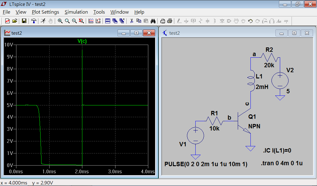
Before you give the answer to the question in the title, could you please tell me whether the BJT in the circuit below will be destroyed by the inductor's large negative voltage when the switch is opened? I mean when a large voltage is applied between the collector and the emitter while the base is floating, will a BJT be destroyed?
upload_2015-6-4_22-23-27.png

Here's what I know: at time of 2ms, when the switch is opened, the inductor is trying to maintain its current by giving a large negative voltage which is applying between node c and ground. There are capatances between B-C and B-E junctions of the BJT, when leaving the base not connecting to anything, only a large voltage between C and E would cause damage to the BJT? If so, how does it work?

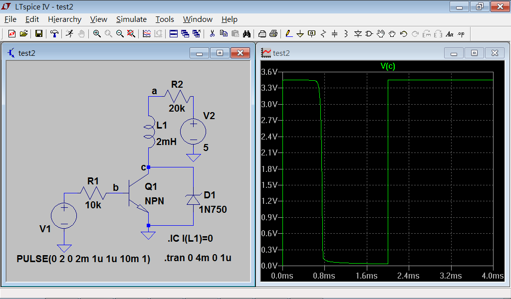
When I add a zener diode in parallel with the BJT, the 1N750 has a berakdown voltage 0f 4.7V at a testing current of 20.245mA,
upload_2015-6-4_22-47-18.png

will it work?

Thank you.
 
Yes, many a transistor has been destroyed by inductive spikes.
You can use a zener from the collector to ground but it should have a breakdown voltage greater than the supply voltage or it will conduct all the time (if you check D1's current in your simulation you will see this).
For your simulation it should have a breakdown greater than 5V.

Alternately you can put a standard diode across the inductor (cathode to supply side). This will provide a path for the inductor current when the transistor turns off and prevent any spike.
Thank you very much crutschow. I understand it now.
 
The inductor does NOT cause a negative voltage at the collector of the transistor when it is turned off. The voltage spike is positive and is only +9.6V that will not harm the transistor. Usually an inductor causes hundreds of volts.

The base of the transistor should never be not connected to anything. Its drive is +2V or 0V through the 10k resistor.
 
The inductor does NOT cause a negative voltage at the collector of the transistor when it is turned off. The voltage spike is positive and is only +9.6V that will not harm the transistor. Usually an inductor causes hundreds of volts.
At the collector of the transistor, it experiences a positive voltage when the current is cut off. For the reference directions shown below, the inductor's voltage is turned to negative when the BJT is turned off, because di/dt < 0.
upload_2015-6-7_12-29-31.png


The base of the transistor should never be not connected to anything. Its drive is +2V or 0V through the 10k resistor.
Considering a transistor seperately, if the base did not connect to anything, only a large enough voltage were applying between the collector and the emitter, would it cause damage to the transistor?

A large voltage may destroy a capacitor, there are tiny capacitances between collector-base and base-emitter junctions, so I thought maybe they would "blow up" if a large enough voltage were across them.(?)
 
At the collector of the transistor, it experiences a positive voltage when the current is cut off. For the reference directions shown below, the inductor's voltage is turned to negative when the BJT is turned off, because di/dt < 0.
I agree that the collector has a positive voltage spike but I do not agree that the inductor's voltage is turned to negative.

Considering a transistor seperately, if the base did not connect to anything, only a large enough voltage were applying between the collector and the emitter, would it cause damage to the transistor?
It probably would never happen to have the base disconnected from its driver and if it happens then the transistor would turn off slowly maybe eliminating a voltage spike. But if the collector goes positive then the base-collector capacitance and stray wiring capacitance would feed some positive base current. This current would cause the transistor to try to conduct that might cause it to momentarily overheat. The base current might slow down and reduce the voltage of the collector voltage spike.

A large voltage may destroy a capacitor, there are tiny capacitances between collector-base and base-emitter junctions, so I thought maybe they would "blow up" if a large enough voltage were across them.(?)
The base-emitter voltage drop cuts the voltage across the tiny capacitances.
 
I agree that the collector has a positive voltage spike but I do not agree that the inductor's voltage is turned to negative.
...........................
It depends upon how you look at the inductor polarity.
When you are applying voltage to an inductor, the terminal where the current enters is positive with respect to the terminal where the current exits.
When you remove the voltage source then the inductance cause the exit terminal to become positive with respect to the entrance terminal, a reversal of polarity across the inductor.
But, of course, the voltage across the transistor stays positive for both scenarios.
 
It depends upon how you look at the inductor polarity......
I understand what you mean. The collector terminal of the inductor goes negative when the transistor conducts and the flyback voltage makes it go positive (well above the power supply voltage) when the transistor is turned off.
 
Vceo, one of the parameters of a BJT, the breakdown voltage under common emitter configuration with base open-circuited.

If we apply a voltage larger than Vceo of a BJT between the collector and the emitter with the base open-circuited, will it cause damage to the BJT?
 
Manufacturers say that if you exceed maximum ratings then damage can occur. They call it "breakdown". A transistor part number has a listed maximum voltage that some transistors will have breakdown at but others survive voltages a little higher.
I think breakdown causes a transistor to avalanche and suddenly conduct current. The voltage and current cook its chip.
 
Vceo, one of the parameters of a BJT, the breakdown voltage under common emitter configuration with base open-circuited.
Many of the big power transistors I have used have two different breakdown voltages.
There is the voltage with the base at 0 or negative voltage.
There is a lower breakdown voltage if the base is anything positive. (0.3 volts for example)
 
If the base is open (not connected to anything) then the collector to base leakage current is amplified and collector to base capacitance (plus stray wiring capacitance) causes the transistor to conduct at a lower voltage and conduct quickly.
The heating caused by the voltage and current causes the leakage current to increase which also speeds the breakdown.
 
With 20k series resistance it would have to be a hell of a spike to damage the transistor.
Which an inductor can readily generate.
 
Here is something I did to illustrate this principle way back in 2006....

snubb.gif

snubb1.gif
 
Status
Not open for further replies.

Latest threads

New Articles From Microcontroller Tips

Back
Top