Fluffyboii
Active Member
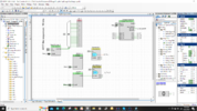
For a long time being unable to easily create a singular pulse, simulating something like a button press annoyed me. For example: I have two CD4017 chips in a sequencer. One of them is driving LEDs while other is used for logic signals. I did this because I did not want to bother with transistor buffers at each output. Both share same clock and reset inputs. But because we live an flawed World these chips are not in sync when the circuit is first powered on. LEDs and logic outputs don't match unless I give a positive reset signal at least for once. Even though this is not the end of the World it is very inconvenient. Yet I can't find a way to automate it.
Lets say I used the clock signal of the sequencer with a latch. Now I have a constant positive signal at latchs output. How will I make it a pulse though. Do I need another clock signal to pull the enable pin of the latch low, after that. Digially making this would require lots of work. In fact I already put more work into making two CD4017 work together inatead slapping some bjt buffers at the outputs already.
Or lets say I want a monolitic timer with NE555. But I want it to start as soon as when the circuit is powered on instead of connecting a button to trigger pin. There is no way of doing it as much as I know.
And while having the CS class about logic gates it always bothered me that there was not a clean way of having a "delay" gate of some kind. I mean you can use multiple gates and sequencal components to have the same effect but there are not a single prebuild, easy to apply delay option. Which usually makes things more complex than it should be.
I think some transistor magic should be able to create what I want. Sadly I can't wrap my head around analog mathematics rabbit hole. I can't do the calculations in order to design a realiable circuit lile that.
Last edited: