Continue to Site

Welcome to our site!

Electro Tech is an online community (with over 170,000 members) who enjoy talking about and building electronic circuits, projects and gadgets. To participate you need to register. Registration is free. Click here to register now.

  • Welcome to our site! Electro Tech is an online community (with over 170,000 members) who enjoy talking about and building electronic circuits, projects and gadgets. To participate you need to register. Registration is free. Click here to register now.

How to connect patch antenna to digital ground?

Status
Not open for further replies.

maryammagdy

New Member
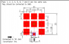
I'm struggling with antenna connections to GPS module in my PCB design. My antenna is a smd passive patch antenna, "SGGP.25.4.A.02 from Taoglas". The antenna shape and recommended footprint is in the first two pictures. I'll be adding an antenna ground plane directly underneath the antenna. I'm confused about the digital GND pads (1 to 9 in second picture) of the antenna connections, I'm guessing they need to be connected into the digital gnd layer I have on layer 2 through lots of Vias? with copper keepout regions between the ground pads and surrounding the feedline?


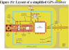
The third picture is the only patch antenna layout I've managed to find from Abracon patch antenna application note but it's for an active antenna. Their design is confusing me greatly and it doesn't seem right to me. They don't have an antenna gnd plane underneath the antenna. I'm guessing the yellow region is a digital ground (separated from the ground of other components) and they're connecting the ground pads of the antenna to the ground of the GPS receiver through traces. If I connect the gnd pads this way I'll have an interrupted antenna ground plane.
 

Attachments

  • Capture.PNG
    Capture.PNG
    179.4 KB · Views: 222
  • jnbio.png
    jnbio.png
    75.7 KB · Views: 222
  • iohopi.png
    iohopi.png
    289.9 KB · Views: 224
The pads will presumably have vias or clusters of vias linking them to the ground plane layer, which forms the other element of the stripline RF connection (on another layer).

I'd expect the ground is split in to small pads to control solder flow during assembly; a single large area could allow solder to flow where its not wanted.

Start by working out the 50 Ohm stripline geometry for the PCB thickness & layers you are using, then work in the ground connections for the antenna.
 
They don't have an antenna gnd plane underneath the antenna.
the antenna connection is on the left side, and looks like it goes to a SMA connector, so the antenna isn't part of the PC board. the digital and signal grounds should be kept separate.

there isn't a shortage of DIY GPS antenna designs on the web, as you can see [here]
 
Thanks for comments. Someone somewhere else have been telling me to ignore the Abracon figure since it has nothing to do with my antenna. I kinda confused digital ground and antenna grounds I guess.
I have another question please. What about the GPS receiver's ground? It is a digital ground but it better be separated from MCU's ground right? But shall it be separated from the antenna's ground on the second layer? In other words, How should I construct my ground plane which is on the second layer of my 4 layer PCB? I will be having an antenna ground on the top layer directly beneath the antenna.
 
Last edited:
Look at the data for the receiver module you are connecting the antenna to.

That should have details of the RF input arrangement, how the stripline terminates and what ground is used.
Then work back from that.
 
Status
Not open for further replies.

Latest threads

New Articles From Microcontroller Tips

Back
Top