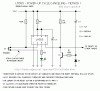
Think of it slightly differently. The negative end of the capacitor is clamped one diode drop (≈0.65V) below ground. Ground is always ground

Because you cannot change the voltage on a capacitor in zero time, right after the input to the supply is turned off, C1 (and the filter capacitor in the powersupply) holds Vcc at almost the previous supply voltage. C1, and the supply's filter caps slowly discharge toward ground. When the dust settles several seconds later, C1 and the supply's filter capacitor are both left discharged...