Continue to Site

Welcome to our site!

Electro Tech is an online community (with over 170,000 members) who enjoy talking about and building electronic circuits, projects and gadgets. To participate you need to register. Registration is free. Click here to register now.

  • Welcome to our site! Electro Tech is an online community (with over 170,000 members) who enjoy talking about and building electronic circuits, projects and gadgets. To participate you need to register. Registration is free. Click here to register now.

How does this telephone “dock” work?

Status
Not open for further replies.

Athosworld

Member
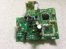
I have this telephone dock I teardowned and found that apparently, it is powered with 9 volts AC that seems to be rectified to DC.

There is something blobby going in the upper right, I decided to decap the chip.
The die photos:
E87A80A9-4183-4C5E-B808-B8FC36EB2EF0.jpeg
FE4C8EC7-6A23-44FB-A671-CE0ED385BFFF.jpeg
 

Attachments

  • 9BC51B3C-0391-4931-BBEA-C179505DBD71.jpeg
    9BC51B3C-0391-4931-BBEA-C179505DBD71.jpeg
    1.4 MB · Views: 188
Most likely a dedicated DECT base controller such as these


Or just a DSP class microcontroller.

The board was made to take a conventional 100 pin flat pack TQFP style IC as an alternate to the COB construction, likely either for initial production and design proving or just as an alternate depending on what IC sources were available.

You can learn infinitely more from the ICs that have numbers than from "blobs"!

And you can learn nothing practical or useful for designing your own stuff by pulling ICs apart, whether normal package or bare die..

Other than the controller IC:
The area at the lower left of the PCB is the telephone line interface, middle area power supply & voltage regulation, lower right corner the radio [DECT] transceiver IC.

The top centre area with the TO92 transistors is likely audio amplification or buffering between the phone line interface and ICs.

And the 8 pin at the top right most probably a memory IC, either settings storage or voicemail (or both) depending on its capacity.

The photo is not good enough quality to read the part numbers.
 
Last edited:
For comparison - this is the board from a Siemens DECT base, a bit better quality with a fully screened RF section.

Note the similar 100 pin main controller at the top right, with the 8 pin memory IC next to it; very possibly the same IC as was in the wrecked one...

The circuitry is roughly similar, just more compact components with packaged bridge rectifiers and mostly surface mount, rather less discrete components.

Gigaset_PCB.jpg
 
Status
Not open for further replies.

Latest threads

New Articles From Microcontroller Tips

Back
Top