Continue to Site

Welcome to our site!

Electro Tech is an online community (with over 170,000 members) who enjoy talking about and building electronic circuits, projects and gadgets. To participate you need to register. Registration is free. Click here to register now.

  • Welcome to our site! Electro Tech is an online community (with over 170,000 members) who enjoy talking about and building electronic circuits, projects and gadgets. To participate you need to register. Registration is free. Click here to register now.

High power adjustable switching power supply (SMPS) 3-60V 40A Help

Status
Not open for further replies.

richiewillmott

New Member
Hi,

I'm looking for some help on this Adjustable SMPS Circuit found on Danyk.cz,

reg60v.png


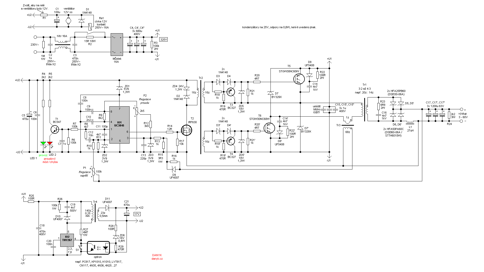
I've built the circuit on a PCB and everything works fine Voltage regulation etc...

But as soon as I attach a load (A 60 Watt 12V Light Bulb) in this case, the IGBTs short out and die, all 3 legs are shorted together.

I tried with 600v Mosfets as well but the same still happens.

It's not on the PCB I designed, but I have soldered RC Snubbers accross the IGBTs

BX4fHs4.png


Any Help would be much appreciated.
 
Welcome to ETO!
I don't see any provision in that circuit for dead-time to ensure one IGBT turns off fully before the other one turns on. Depending on how the feedback works to control the pulsing of T2, that might result in greater average shoot-through current through T5 and T6 when the circuit is driving a significant load than when it is idle.
 
Hi Ronsimson,

Yes both IGBTs turn on together in a Two Switch Forward converter, anyone any ideas why the IGBTs keep blowing when under light load though?
 
I need to see many things. Trouble shooting over the internet is hard.
Do you have an oscilloscope? Maybe the gate voltage is not good. I did not look at the data sheet but 20V is max.
Are the transistors hot? I think they are cold when they die.

Do you have a current probe for a oscilloscope? Maybe there is core saturation on the big transformer.
 
Next time you make a off power line power supply, keep the primary and secondary separated. Pretend there are 2000 volts from P to S.
1575249896668.png

Look at the distance from the pin on P$1 and the red trace on the transistor. This problem is all over the board. Your supply may work just fine but this is not something you can put into production.
1575250410001.png
 
I think theres meant to be some deadtime built into Tr2, one fet turns off while the other fet turns on, Zd4 and d2 are also important to get the transformer working right, the core type is also probably important.
Danyk did get this circuit to work.
Still migth be shoot through though, if you 'scope D9's anode you'll see if this is happening by huge spikes, these might not get back to the control chip because of the filter.
Another possibility is that your circuit has very different frequency response and therefore phase margin than the original making it unstable and its going into wild oscillation then blowing up, does the main power trans make weird noises?
Did you use the same power diodes?
 
Still migth be shoot through though,
Not shoot through. Both transistors are to be on at the same time.

I did not look up all of the power diodes. If they are slow, that will kill the transistors. Reverse recovery time.
 
Your right.
Somehow I thought this was a push pull, but its a 2 trans forward, the gdt is wired in phase so both trans's are on at the same time.
D7 and D7' conduct when the igbt's are off to reset the trans.
So maybe as pointed out check the o/p diodes, then maybe transformer coupling, the gdt should be trifilar wound, and then perhaps the compensation.
The Uc3845 is limited to 50% duty, so the clamp network with Zd4 in it needs to be greater than 1/2 U2 supply voltage to ensure tr2 and tr1 resets.
 
Last edited:
so the clamp network with Zd4 in it needs to be greater than 1/2 U2 supply voltage to ensure tr2 and tr1 resets.
Good call. I checked, supply=17V and Clamp = 24.7. That seems OK.
I think we are wasting out time here. We need much more information. (good pictures of the PCB … thanks)

The BY329X diode seems fast. I would never use a 1500V diode but I think it will be fine. (maybe a slow diode was used)
The four output diodes need to be FAST. What diodes are used?


The first power line switching power supply I worked on: (35 to 40 years ago, looks much like this supply) When the Chief Engineer wound the transformer they would die in exactly 24 hours. It would blow the lids off the transistors. If I wound the transformers they did not die. It took a month to determine the insulation on the wires was not strong. He thought two layers of 850V insulation was good. He used super glue to hold the wires in place and I used tape. While I can't know what is happening on this supply there is Primary to Secondary insulation problems all over the board.
 
I spose if tr1 was wound with incorrect phase this might happen, the thing will rectify magnetization current and maybe even regulate no load, but then saturate tr1 and blow the trannies when a load is applied.
Where mains is concerned I use 5 layers of tape, and put 1/2 the primary on first and the other 1/2 last, and leave a gap at the edges, and have insulation on the leadouts.
Yes trying to diagnose by proxy isnt effective.
 
One thing to be aware of about this supply is that the output is NOT isolated from the input line voltage.

Even though it uses a transformer between the primary and the secondary, the fact that the feedback is directly connected from the output to the control circuitry in the primary defeats the isolation. Output negative is connected to the rectified primary negative.

So even adding some clearance distance on the PCB won't help. The circuit should be changed to provide voltage feedback through an optocoupler or some other isolated method.


This post has incorrect information as pointed out by Nigel.
 
Last edited:
One thing to be aware of about this supply is that the output is NOT isolated from the input line voltage.

Even though it uses a transformer between the primary and the secondary, the fact that the feedback is directly connected from the output to the control circuitry in the primary defeats the isolation. Output negative is connected to the rectified primary negative.

So even adding some clearance distance on the PCB won't help. The circuit should be changed to provide voltage feedback through an optocoupler or some other isolated method.

I suggest you look further at the circuit, specifically the lower left corner! :D

Not that I'm recommending this design in any way.
 
I suggest you look further at the circuit, specifically the lower left corner! :D

Not that I'm recommending this design in any way.
You are correct.
I'm used to supplies that have the PWM control as part of the primary circuit. I did not see that this circuit has a separate, isolated supply for the PWM controller.
 
This post has incorrect information as pointed out by Nigel.
I fell in that trap to. The schematic is hard to follow. Luck me, I hit the edit button before Nigel came along.
Also
The other trap is the "two transistor shoot through" trap.
?Is there another trap? yes, getting sucked down this rabbit hole.
 
Status
Not open for further replies.

Latest threads

New Articles From Microcontroller Tips

Back
Top