Hi,
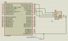
Below is the code to write "8" into SPI eeprom and then read "8" back and store it in "data1". However, "data1" is always 0 no matter what i write to the eeprom. Attached is my circuit in Proteus. Please advice..
Below is the code to write "8" into SPI eeprom and then read "8" back and store it in "data1". However, "data1" is always 0 no matter what i write to the eeprom. Attached is my circuit in Proteus. Please advice..
Code:
#include <p18F4620.h>
#include <delays.h>
#include <spi.h>
#include <usart.h>
#include <stdio.h>

#pragma config WDT = OFF
#pragma config MCLRE = ON
#pragma config LVP = OFF
#pragma config OSC = HSPLL
#define CLOCK_FREQ		(40000000ul)      // Hz

#define CSEE PORTCbits.RC0 // select line for Serial EEPROM

#define SEE_WRSR 	1 // write status register
#define SEE_WRITE 	2 // write command
#define SEE_READ 	3 // read command
#define SEE_WDI 	4 // write disable
#define SEE_STAT 	5 // read status register
#define SEE_WEN 	6 // write enable


void SPIEEPROMInit();
void UARTInit();

int writeSPI( int data)
{
	SSPBUF = data; // write to buffer for TX
	while( !SSPSTATbits.BF ) // wait for transfer to complete
	return SSPBUF; // read the received value
}//writeSPI

void main()
{
        int data1, data2, i;
	SPIEEPROMInit();
	UARTInit();


	// send a Write command
	CSEE = 0; // select the Serial EEPROM
	writeSPI( SEE_WRITE); // send command, ignore immediate data
	writeSPI( 0); // send MSB of memory address
	writeSPI( 1); // send LSB of memory address
	writeSPI( 8 ); // send the actual data to be written
	CSEE = 1; // start actual EEPROM write cycle

	// send a Write command
	CSEE = 0; // select the Serial EEPROM
	writeSPI( SEE_READ); // send command, ignore immediate data
	writeSPI( 0); // send MSB of memory address
	writeSPI( 1); // send LSB of memory address
	Delay10KTCYx(1);
	data1 = writeSPI( 0); // send dummy, read data

	CSEE = 1; // terminate the read sequence, return to low power

while (1);
}

void SPIEEPROMInit()
{
	SSPSTAT = 0xC0; //SPI Bus mode 0,0
	SSPCON1 = 0x21; //Enable SSP,Fosc/16

	DDRCbits.RC7 = 0; //Define CS as Output
	DDRCbits.RC3 = 0; //Define SCK as Output
	DDRCbits.RC4 = 1; //Define SDI as Input
	DDRCbits.RC5 = 0; //Define SDO as Output
	CSEE = 1; // start actual EEPROM write cycle
}


void UARTInit()
{
	SPBRG = 64;
	TXSTA = 0b00100010;
	RCSTA = 0b10010000;
	BAUDCON = 0b00000000;
	TRISCbits.TRISC7 = 1;
	TRISCbits.TRISC0 = 0;
}