Continue to Site

Welcome to our site!

Electro Tech is an online community (with over 170,000 members) who enjoy talking about and building electronic circuits, projects and gadgets. To participate you need to register. Registration is free. Click here to register now.

  • Welcome to our site! Electro Tech is an online community (with over 170,000 members) who enjoy talking about and building electronic circuits, projects and gadgets. To participate you need to register. Registration is free. Click here to register now.

problems with a miso line in spi comunication

bizarro

New Member
Hello fellows,

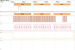
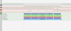
I'm trying to communicate between a microcontroller (master) and a front end device (slave), but when I send commands from master to slave, the MISO line is operating faster than the SCLK line, which is configured to work at a frequency of 500 KHz. Is there anyone who had a similar problem and can share the experience with me to try to resolve this.
Thanks in advance
 
First! the master controls the speed with the clock line ergo, the end device must be configure as a master as well.. This cannot continue for long as the clk line is in contention.

As you haven't given any details to any of the devices, I very much doubt we can help you resolve this
 
Recently had a big debug session with a FRAM (2mb) and a dsPIC33EV256GM304 , This SPI needs careful coding, ( I dont use any library or code help ) my problem seemed to be centered round high impedance on the MISO during the masters MOSI bytes. I had let it float , thought about pull down or up, in the end I just read the SPIBUF and put byte in a 'waste' uint8_t. .. l had to send 3 bytes address , then a dummy byte so the Fram could send its data . Probably not much help.

FRAMRDOK.jpg
 
Last edited:
Firts of all, thanks for all quickly responses...

Ian, my mcu (master device), is a MSP432P401R from texas instruments, and I use the B0 module, the comunications pins are P1.5-SCLK; P1.6-MOSI;P1.7-MISO;and P5.0-CS.
The slave device is ads1292R from texas intruments too.
I have configure the spi from my master device to comunicate with a 3-pin SPI mode device.
 

Attachments

  • Screenshot 2024-10-19 at 13.46.51.png
    Screenshot 2024-10-19 at 13.46.51.png
    32.4 KB · Views: 57
Straight from datasheet
datasheet said:
NOTE: Pullups can be used to avoid unnecessary toggles on the QSSI pins, which can take theslave to a wrong state. In addition, if the SSIClk signal is programmed to steady state highthrough the SPO bit in the SSICR0 register, then software must also configure the GPIO portpin corresponding to the SSInClk signal as a pullup in the GPIO Pullup Select (GPIOPUR)register.

these devices are special as they have Quad SSI modules... Make sure that IF!!! I say if as I don't know, that the ssi clock isn't different between channels..
 
Last edited:
Ian, I can't find the information you shared with me. Are you sure this information is for the MSP432P401R board. Even so, I tried to make some changes to the SPI pins, such as adding pullups to try to guide the pins to the correct state, but to no avail.
 
Look at the interface configuration - some QSPI modes use two (or more?) data bits per clock cycle.

I'm guessing that it's in a multi-bit mode rather than single bit.
 
I have perused the datasheet, Nothing stands out.

Your board will have some software tutorials... However! depending on your programming ability, this board can be programed via the arduino IDE.. A lot easier to get things done..
https://www.energia.nu/ read this... It may be a good starter
 
The problem is you will need the library from that site.. If you can vert from C++ to C ( or even read C+) you can see their set up.

A quick look and every device on that board is catered for.
 
Well, all my code is in C. I think I will have a small problem with the SPI communication and I hoped that I could get some information on this forum that would help me solve my problem.
Code:
#include <msp432.h>
#include "spi.h"
#include "ads1292r.h"

void set_spi(void) {
    initialize_ports();
    initialize_spi();
}

void initialize_spi(void) {


    EUSCI_B0->CTLW0 |=  EUSCI_B_CTLW0_SWRST;        /*EUSCI_B0 INTO RESET MODE*/

    EUSCI_B0->CTLW0 =   EUSCI_B_CTLW0_SWRST         /*KEEP IN RESET*/
                       | EUSCI_B_CTLW0_MSB          /*MSBIT FIRST*/
                       | EUSCI_B_CTLW0_SYNC         /*SYNCHRONOUSE MODE(SPI)*/
                       | EUSCI_B_CTLW0_MST          /*MASTER MODE DEVICE*/
                       | EUSCI_B_CTLW0_MODE_0       /*SPI 3 PIN MASTER MODE*/
                       | EUSCI_B_CTLW0_SSEL__SMCLK  /*CLOCK SOURCE(SMCLK)*/
                       | EUSCI_B_CTLW0_CKPH;        /*CKPL = 0; CKPH = 1*/


    /*SET CLOCK DIVIDER (ASSUME SMCLK = 12MHz/24, SPI CLOCK 500KHz)*/
    EUSCI_B0->BRW = 24;                             /*CLOCK PRESCALER (12MHz/24 = 500 KHZ)*/

     /*SELECT THE PRIMARY MOCULE FUNCTION*/
     /*INITIALIZE PORT REGISTERS, CONFIGURE FOR SPI FUNCTIONALITY*/
     /*P1.5 (SCLK), P1.6 (MOSI), P1.7 (MISO)*/
     P1->SEL0 |= BIT5 | BIT6 | BIT7;                /*SELECT FIRST AND PRIMARY FUNCTION*/
     P1->SEL1 &=~(BIT5 | BIT6 | BIT7);              /*CONFIRM THE SEL1 IS CLEARED TO USE THE PRIMARY FUNCTION*/

     P1->DIR  |= BIT5 | BIT6;                       /*SET THIS PINS LIKE OUTPUT PIN'S*/
     P1->DIR  &= ~(BIT7);                           /*SET P1.7 LIKE A INPUT PIN*/


    EUSCI_B0->CTLW0 &= ~(EUSCI_B_CTLW0_SWRST);      /*RELEASE EUSCI FROM RESET*/
   // EUSCI_B0->IE |= EUSCI_B_IE_RXIE;

    /*IN THE ADS1292R TECHICAL DATED SBAS502C – DECEMBER 2011 – REVISED APRIL 2020 DOCUMENT, THERE IS
     * A NOTE WHERE IS DEFINED THE STATUS OF  SPI CLOCK SETTINGS ARE CPOL=0 AND CPHA=1.*/

    }

void initialize_ports(void) {
    /*P2.4 - CLK_SEL*/
    /*P2.5 - START*/
    /*P2.6 - POWER/RESET*/
    /*P5.0 - CS*/

    /* GPIO PINS ADS COMMAND PIN'S I/O */
    P2->DIR |= BIT5 | BIT6 | BIT4;          /* START, RESET AND CLK PIN OUTPUT */
    P2->OUT &= ~(BIT5 | BIT6);              /* START AND RESET PINS LOW STATE */
    P2->OUT |= BIT6 | BIT4;                 /* CLK AND RESET PINS TO HIGH STATE*/

    P5->SEL0 |= BIT0;
    P5->SEL1 &= ~(BIT0);
    P5->DIR |= BIT0;                        /*SET P5.0 CS SELECT OUTPUT */
    P5->OUT |= BIT0;                        /*SET P5.0 CS SELECT OUTPUT */

}
 
OK, so that MCU does not have Quad SPI, so what I said earlier is not relevant.

The one thing is does have that could mess things up is Port / Pin mapping - peripherals connections can be routed to any during the program configuration.

From a quick look at the datasheet and your program, it looks like you are doing some mapping - but have not unlocked access to the mapping registers? See section 13.2.1 in the data sheet you linked to?

I'm not familiar with that MCU so I'm not sure if that is related - but it's the only thing that stands out as a possible cause of the problem.
 
As JRW said.. I am also unfamiliar with that device... If there is pin mapping then that isn't in your routine.
I would need to read the datasheet but at this moment I have no time..
 
As mentioned above, try the Arduino IDE to check the SPI functioning - just write a small routine to read/write via SPI and prove if it works or not. Assuming it does, then study the settings used by the Arduino code - and steal them :D
 

Latest threads

New Articles From Microcontroller Tips

Back
Top