Continue to Site

Welcome to our site!

Electro Tech is an online community (with over 170,000 members) who enjoy talking about and building electronic circuits, projects and gadgets. To participate you need to register. Registration is free. Click here to register now.

  • Welcome to our site! Electro Tech is an online community (with over 170,000 members) who enjoy talking about and building electronic circuits, projects and gadgets. To participate you need to register. Registration is free. Click here to register now.

Help With PCB layout

Status
Not open for further replies.

kssoin

New Member
Hello Folks,
I have been following posts on pcb/design/etc.
Recently I made a timer on a gen strip pcb.
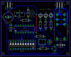
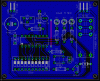
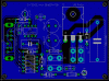
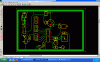
Simply this is a timer using a 4060.As it has been configured for my use a relay switches on after 35 mins approx and then deactivates after the same time. this is repeated till the timer is switched off. The credit for this circuit is to Ron J. I want to use this to switch the charger of my laptop for the longevity of the Li-ion battery.

After downloading ExpressPcb. I have made the schematic and the layout.
The routing has become very complicated. This the first time i am using this software. Many Forum members are using this software. I request your help in sorting out the mess on the pcb.
I am attaching pdf .sch and .pcb files for in a zipped folder. I will appreciate your inputs on this
View attachment TIMER.zip
Best Regards
Kssoin
 
Last edited:
were you planning a single sided board or is double sided ok?

Well, now that I've looked at it, obviously you were thinking of single sided. Your layout did not make sense to me so I did my own version, shown below. Here are some tips for designing this sort of thing:
- place components so that connections are as short as possible, starting with those that naturally group together. For example, I started by putting U1 in the middle, then putting R3, C3, R5 and VR4 close to the pins they connect to. Turn them around so that connections are short. Next, place the dip switches and be prepared to reassign the connections for easiest routing. I didn't need to.
- put a ground around the outside so that any connections to ground go outwards and away from the clutter
- place the bypass caps for the IC near the IC vcc pin
- keep traces running either vertical, horizontal or at 45 degrees for a tidy appearance.
- always maintain minimum of .010 clearance between unconnected copper

It is obvious that you did not try very hard to position components for shortest connections. You need to think as you place each part, and not only move them, but also rotate them to shorten the connections as much as possible.

Here is my version (if you post again I will post the design file of this).
 
Last edited:
Here it is. I don't guarantee I've made all connections so if you use this, check it carefully.
 

Attachments

  • RRversion.GIF
    RRversion.GIF
    64.1 KB · Views: 551
Last edited:
Hello RadiRon,
I immensely appreciate your help. The layout is an eye opener. A magnificent improvement to the one I posted. Please post the .pcb file.
Thanks once again.
Best Regards.
Kssooin
 
Here is my PCB design.

It uses one wire jump, but I guess it is populated more densely. :)

Board size is 2.7750 X 2.2500 inches.

Boncuk

Please recheck your connection of R2/D2. They are connected to the timing capacitor. I guess that LED should be the power indicator. I connected it to a DIP-10 switch to switch it on and off on demand.
 

Attachments

  • 4060-TIMER.gif
    4060-TIMER.gif
    30.4 KB · Views: 928
Helo Boncuk,
Makes the pcb much smaller.
I must acknowledge you and RadioRon for your help. Your commitment to this work is great. I will be etching the circuit using the toner transfer method.
Thanks once again.
Kssoin:)
 
Last edited:
Here is my design file in the attachment. I must admit, Boncuk did a very nice job on his version.
 

Attachments

  • layout.zip
    28 KB · Views: 206
Last edited:
Hard to believe!!

both designs are the same circuit but look totally different.
Boncuk has a very compact layout and Radioron has a layout that is easier to understand. not all jumbled together.
these two boards are prime examples of proper pcb layouts.
I like radiorons idea of the ground trace going around the board. going to have to try that.
one of these days I hope to finish the 5 band specturm analyzer/graphic EQ/with display.
design has been modified at least ten times.
after seeing these two excellent pcb designs I am going to modify again maybe??.
GREAT WORK both of you

Hi MrDEB,

I suppose you overlooked a detail on my PCB design.

Looking at the picture of the first post you will see a thin line surrounding the entire board.

Today you will see the magic of the thin line after "ratsnesting". :D

Regards

Boncuk
 

Attachments

  • TIMER.gif
    TIMER.gif
    32.4 KB · Views: 518
Last edited:
Looking at the picture of the first post you will see a thin line surrounding the entire board.

Today you will see the magic of the thin line after "ratsnesting". :D
I prefer a layout where the open areas are flooded with ground plane, as you show. Not only does this generate a good ground connection, but it minimizes the amount of copper that requires etching, saving etching solution.

I believe "ratsnest" refers to the board layout showing the connections as straight lines directly between nodes, before the traces are generated. Not sure that term applies to the thin line around the board.
 
Yes, flooding the available area with ground pour is something I do as a normal habit on finished boards and I endorse Boncuk's suggestion.

Watch out for the clearances around the relay contacts as we don't know if the OP is planning on running 120V through those. I would clear those a bit more, but that's nitpicking. Good job.
 
@crutschow

In Eagle there is a tool called ratsnest that will reset all the air-wires (rubber bands) to make them as short as possible. It also will cause regions marked as fills (ie ground planes) to flood. The polygon tool marks the area. RatsNest fills it in.

3v0
 
I believe "ratsnest" refers to the board layout showing the connections as straight lines directly between nodes, before the traces are generated. Not sure that term applies to the thin line around the board.

Hi Carl,

concerning groundplanes "ratsnest" fills the entire board with ground after having drawn a polygon using layer16 (bottom layer). The same applies drawing a polygon using layer1 (top layer).

The distance between traces and pads is dermined by the settings in the autorouter (standard 0.2032mm). If you change that value for a greater distance, adapt those values for the DRC - otherwise DRC will stop after 50 errors. You might want to increase the max error count to 5,000. :D

Here is an example using a ground plane with several adjacent ground fills (polygons) to have T1(D), D4, and C5 separated because of HV back EMF.

When drawing more than one polygon it is important not to draw two overlapping ones.

Drawing the outlines with trace width 0 and layer20 (Dimension) prior to drawing a polygon using any copper layer you can make sure not to "overshoot".

You might as well use layer21 (component layer), but hiding top and bottom layer will still leave the components on screen making it hard to erase a line.

If you don't click accurately on a line Eagle assumes you want to delete a component and tells you to do that in the schematic. :)

When done hide all layers except for the dimension layer and delete (erase) the artwork within the board.

Regards

Hans
 

Attachments

  • E-FENCE.gif
    E-FENCE.gif
    32.1 KB · Views: 236
Watch out for the clearances around the relay contacts as we don't know if the OP is planning on running 120V through those. I would clear those a bit more, but that's nitpicking. Good job.

Hi RadioRon,

I didn't intend to "sell" that board as a final design. I would not call it nitpicking to have mains close to circuit ground and not trying to avoid it. :)

Please refer to the next post showing a wider empty space for a potential HV back EMF trace. That thing is connected to the primary winding of a car ignition coil.

Regards

Boncuk
 
Status
Not open for further replies.

Latest threads

New Articles From Microcontroller Tips

Back
Top