Continue to Site

Welcome to our site!

Electro Tech is an online community (with over 170,000 members) who enjoy talking about and building electronic circuits, projects and gadgets. To participate you need to register. Registration is free. Click here to register now.

  • Welcome to our site! Electro Tech is an online community (with over 170,000 members) who enjoy talking about and building electronic circuits, projects and gadgets. To participate you need to register. Registration is free. Click here to register now.

Help with PC board design

Status
Not open for further replies.

trident9

New Member
Greetings

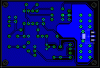
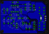
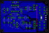
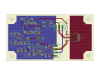
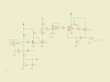
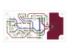
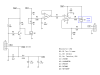
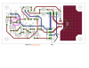
This is my first attempt at designing a PC board, your help in correcting errors will be much appreciated. The input signal is 25kHz PWM from an open drain output. Maximum power dissipation in the pass transistor will be 2 watts for 1 second or less at start-up, continuous dissipation will be 1 watt or less. The gate resistor is purposely large to limit the output slew. The board will be 1 oz copper on both sides.
1) Will the heat sink be adequate for 30 degrees C ambient in still air?
2) Will RFI from input transistor switching be an issue?

Thanks in advance for you help.
_______
trident
 

Attachments

  • Intgr_LM358_pcb.png
    Intgr_LM358_pcb.png
    52.9 KB · Views: 538
  • Intgr_LM358_sch.png
    Intgr_LM358_sch.png
    17.9 KB · Views: 502
Hi Trident9,

first off, I guess the PCB can neatly be done single sided with Q3 mirrored onto the solder side.

If you can afford to have more space try to enlarge the heatsink plane.

Further I see "FG" on two connectors, bot not elsewhere in the schematic. What is it good for?

Boncuk
 
Q3 where is it??

nice layout but no need for 2x board
just 1 or 2 jumpers
 

Attachments

  • pcboard.PNG
    pcboard.PNG
    53.2 KB · Views: 390
Q3 is located on top of the cooling pad. :)

Zoom it.
 
first off, I guess the PCB can neatly be done single sided with Q3 mirrored onto the solder side.

If you can afford to have more space try to enlarge the heatsink plane.

I missed Q3 but mirriring is solution
 
Can someone point me to info for designing thermal pads as to the area required? How many and what size via are appropriate?

Any opinions as to how much radiated noise Q1 and Q2 may generate, would a ground plane under U1 be an effective shield?

Thermal pad for Q3 is double sided to minimize the board size, currently there is a little more than 0.65 sq inch on both sides of the board. FG is a signal from the load that needs to go back to the controller.
_______
trident
 
Hi trident9,

I have reworked your circuit with a large cooling surface for Q3 including 14 thermal drills.

Board size is 57.4675X39.6875mm (2.2750X1.5625").

It's fully single sided and uses two fills, ground fill on the left hand side and drain Q3 fill on the right hand side.

I'd be interested to know how much drain current you use for Q3.

With the given dimensions of the cooling pad the temperature will be about 45deg/C at max current.

Boncuk
 

Attachments

  • GND-FILL.gif
    GND-FILL.gif
    23.6 KB · Views: 340
  • DQ3.gif
    DQ3.gif
    23.8 KB · Views: 227
  • LM358-CIRCUIT.gif
    LM358-CIRCUIT.gif
    30.9 KB · Views: 900
Hi trident9,

I have reworked your circuit with a large cooling surface for Q3 including 14 thermal drills.

Board size is 57.4675X39.6875mm (2.2750X1.5625").

It's fully single sided and uses two fills, ground fill on the left hand side and drain Q3 fill on the right hand side.

I'd be interested to know how much drain current you use for Q3.

With the given dimensions of the cooling pad the temperature will be about 45deg/C at max current.

Boncuk
Nice and cute board Boncuk!! Which artwork do you use?
 
Hi Sarma,

there is no artwork program used. It's simply Eagle schematic and board design software.

I used the OP's original PCB layout and did a few changes to avoid wire jumps. (also moved the SMD transistor to the solder side.)

Regards

Hans
 
Thank you, MrDEB,

I didn't find out what it is good for (missing connections), but here is what the OP planned it to use for:

FG is a signal from the load that needs to go back to the controller.

Boncuk
 
Greetings mneary
The board will be vertical in still free air @ 30 degrees ambient, the ambient temp will be constant. From the Fairchild data-sheet: thermal resistance from junction to case is 12 degrees C per watt. Max junction temp is 150 degrees C. Referencing the transient response curve, transient resistance would be 0.2 for a single 1 second pulse. If I am understanding the math correctly a thermal pad that can dissipate 1 watt continuous would be able to dissipate a single 5 watt 1 second pulse. I would like to error on the safe side using 125 degrees C as the max. junction temp. and 35 degrees C as the ambient. What I do not have is a value that relates area to thermal resistance for a double sided 1 oz copper thermal pad to plug into the equation.

Greetings Boncuk
I much appreciate you posting the alternate layout. I am approaching this project as a learning opportunity. If someone does all the work for me that opportunity will be lost. I am using EAGLE 5.6.0 with custom package outlines, If you like, I can post the files. I will not be etching the board myself, so going double side is not an issue. Max. current would be at 1/2 Vss, ~330mA @ 6 volts.

How did you calculate the thermal rise for Q3? also your layout does not address several items I believe are important: 1) A low impedance ground path from J1 to J2 for load power, 2)The gate resistor for Q3 should be as close to the transistor as possible, 3) no trace for the FG signal.
_______
trident
 
Last edited:
How did you calculate the thermal rise for Q3?

I very seldom calculate. Just used the data sheet and the suggestions for the thermal pad according to size and copper weight and estimated the resulting temperature. According to my experience my estimates are close to calculated ones, saving headaches. :)

also your layout does not address several items I believe are important: 1) A low impedance ground path from J1 to J2 for load power, 2)The gate resistor for Q3 should be as close to the transistor as possible, 3) no trace for the FG signal.

1) A low ground impedance is given by the ground fill. 300mA is just laughably low.

2) I moved the gate resistor towards the gate, but I think this has absolutely no effect on the function. If you are afraid that noise will be the problem it could be inserted in the trace between the OpAmp and the resistor.

3) If you had labelled the traces instead using flags I'd known they must be connected in the schematic and on the PCB. They are connected now using a wire jump.

Boncuk
 

Attachments

  • LM358-CIRCUIT-01.gif
    LM358-CIRCUIT-01.gif
    31.8 KB · Views: 862
Last edited:
Greetings
Have been reading everything I can find concerning SMT thermal pads and discovered that R(th)JA is difficult to predict because it consists of several parallel paths whose impedance varies as the heat flux changes. I did discover a few rules of 'Thumb' in the process:
1) The lowest R(th)JA is provided by a continuous pad centered around the component, on the same side as the component.
2) Increasing the thickness of the copper pad improves R(th)JA significantly.
3) Pads larger than 1 sq inch do not significantly improve R(th)JA.
4) Multi-layer boards improve R(th)JA.
I have reworked the board with a Dpak MOSFET and moved it to the center line of the board. The positive rail routing in Boncuk's layout gives shorter traces and I've incorporated it as well. Thank you Boncuk
_______
trident
 

Attachments

  • Intgr_LM358_Dpak_pcb.png
    Intgr_LM358_Dpak_pcb.png
    52.6 KB · Views: 312
  • Sch.png
    Sch.png
    26.3 KB · Views: 191
Last edited:
Did you read to put thermal drills underneath the transistor you want to cool?

From my understanding thermal drills take care of air movement, hence improving cooling. If they are blocked there won't be any air movement.

Using double layer copper with plated thermal drills both the component side and the solder side serve as cooling pad.

On the other hand you could use a single sided board with 2oz of copper weight as suggested by the manufacturer.

Boncuk
 
Greetings Boncuk
I did not find any information on using thermal drills (via) for air circulation through the board. Can you point me to an article? In the last design the via are to increase the thermal transfer between the top pad and bottom side pad, so they are close to the hot spot created by the MOSFET, but not inside the solder area for the MOSFET, except for the center via I'm using for manual soldering.
_______
trident
 
Last edited:
Status
Not open for further replies.

Latest threads

New Articles From Microcontroller Tips

Back
Top