Continue to Site

Welcome to our site!

Electro Tech is an online community (with over 170,000 members) who enjoy talking about and building electronic circuits, projects and gadgets. To participate you need to register. Registration is free. Click here to register now.

  • Welcome to our site! Electro Tech is an online community (with over 170,000 members) who enjoy talking about and building electronic circuits, projects and gadgets. To participate you need to register. Registration is free. Click here to register now.

Help with designing PCB with 433MHz helical wire antenna

Status
Not open for further replies.

Kian

Member
Hi all,

I am trying to design my own pcb based on the CC1310 wireless MCU from TI. I am using it for 433MHz communication. I want to use a helical wire antenna for my application.

There is too much info out there and seems like every website/article talks about a different thing and I am really confused about what are the PCB requirements. I want to achieve a max transmission range of about 150 metres.

Here are my questions:

1. I read that a 4 layer PCB is recommended because I have an entire layer as the ground plane. But is this really necessary? A 4 layer PCB will add to the manufacturing cost.

2. I read that the antenna needs to have a certain clearance from the ground plane. How do I know how much clearance I need? And I never see this large empty space in those compact RF modules. So is it really necessary?
zzy8pme.jpg

3. A PI matching network is recommended and a 50 ohm PCB track should be connected to the antenna. Where should the 50 ohm PCB track start from?

4705.cc13xxem_2D00_7xd_2D00_4251_5F00_1_5F00_1_5F00_0.jpg

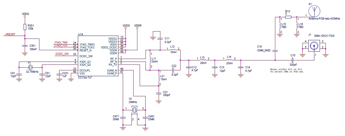
Should the 50 ohm line start from after L14? Or after C16?
 
The data sheet for the CC1310 says "The board layout greatly influences the RF performance of the CC1310 device." I think that "greatly influences" is an understatement.
A full ground plane on the board does several things
1) simplifies all return paths for digital switching currents, meaning current loops are much smaller than if you don't use a groundplane. This minimizes the ability of the digital noise generated by on-board logic to degrade your sensitive receiver
2) lowers the impedance of all interconnects on the board, resulting in less undesired coupling, additionally supporting your goal of a quiet environment for your receiver
3) improves the counterpoise against which your antenna is operating as a monopole. A full board ground plane will provide a greater ability to push power out of your transmitter as a result.
4) reduces undesired spurious emissions
5) supports your 50 ohm transmission lines (although a full board plane is not necessary just for this reason)
and probably some other good reasons.
Let's face it, to be in the RF game, you have to use ground planes. That doesn't mean a 4 layer board, but it is pretty hard to do it on a 2 layer board because you are forced to do all your interconnects only on the top layer.

The clearance of the wire coil from the ground plane is what you might call a soft parameter. You can get away with less, but your range of communications will likely drop also. If you are shooting for absolute maximum possible range, you have to optimize the antenna performance and spacing it further from the ground plane, up to a critical dimension, does this. The designers of those compact RF modules are all choosing their own compromise on board area vs range. Without an EM simulator to help you make a choice, you will have to rely on principles and rules of thumb. The image you included in your post shows a reasonable spacing from ground plane to the coil section.

The antenna that you show in your post begins at the edge of the ground plane. The trace that goes from that edge up to the coil of wire is part of the antenna. The 50 ohm trace should end at the edge of the ground plane, where the antenna starts. The other end of the 50 ohm track is the point where the impedance matching circuit or low pass filter circuit ends, or in other words, at the junction of L14 and C14. The schematic includes some optional antenna matching components, L15, R13 and L16. These should be placed between the 50 ohm trace and the antenna trace, right at the edge of the groundplane.
 
Last edited:
I want to expand on my point 3 above. Antennas on these kinds of boards are almost always some sort of monopole or modified dipole. The part that you call the "antenna", being a trace and a coil of wire in your example, is really only half of the antenna. The other half of the antenna is all the other circuitry and area of ground plane, the part that you might call "everything else" and I call the Counterpoise. When your transmitter pushes power out to the antenna, the current that flows on the antenna is matched by an opposing or balancing current on the counterpoise. So, in effect, the entire assembly forms a sort of dipole where one half is skinny and the other half is wide. The bigger/longer you make these two halves, the easier it is to resonate them at lower frequencies such as 433 MHz and the better the board radiates.

One side affect of this is that your digital circuits are actually embedded into the antenna by virtue of their being mounted on the counterpoise. Those readers out there that know about how digital circuits generate high frequency noise will appreciate that there is no worse place to put a digital noise generator than on the antenna itself when building a transceiver. Practicality requires that we must because people don't like things to be so big, so it behooves you to make the digital stuff as quiet as possible. A ground plane is essential in this.
 
Last edited:
A normal mode helical antenna like this is full of compromises.

1 It has significant loss compared with a simple monopole above a groundplane.
2 Placing the antenna within the equipment results in a less than ideal radiation pattern.
3 Without test equipment to measure the antenna, it is impossible to determine the resonant frequency and feed impedance of the antenna. These parameters will be affected considerably by the physical environment (including non-conducting materials) around the antenna.
4 The random relative orientation of the antennas at each end of the link can result in considerable (20 to 30dB) additional path loss.

The best thing that I can suggest is that you try it.
If it works, great, be happy.
If it does not work, use a more formal antenna (eg dipole, quarterwave groundplane or...) at each end of the link.

JimB
 
Thanks RadioRon and JimB.

RadioRon,

You mentioned that the antenna begins at the edge of the ground plane. Does this then add to the length of the antenna? I presume the helical wire antenna is already at the correct length. Doesn't think extra PCB trace from edge of ground plane to the actual antenna add extra length to the antenna? Instead of it being a curved track, can i just move the PI network to the right edge of the PCB and have a straight track going straight up to the antenna? And how do I determine the width of this PCB track?

I am thinking of something like this:

v4XtPdn.jpg


The antenna that you show in your post begins at the edge of the ground plane. The trace that goes from that edge up to the coil of wire is part of the antenna. The 50 ohm trace should end at the edge of the ground plane, where the antenna starts. The other end of the 50 ohm track is the point where the impedance matching circuit or low pass filter circuit ends, or in other words, at the junction of L14 and C14. The schematic includes some optional antenna matching components, L15, R13 and L16. These should be placed between the 50 ohm trace and the antenna trace, right at the edge of the groundplane.
 
Last edited:
Yes, the trace adds to the length of the antenna. Yes, you can put the pi network at the right side and just make the track straight, that will work fine. The width of the straight track is not terribly critical and you can choose any practical width that will be easy to etch, but don't get carried away and make it really fat either. The range of 0.03 to 0.07 inch width should be fine. The width doesn't affect losses very much because most of the current will flow at the edges of the trace and the edges don't really change much with thinner or wider traces. The width does have an affect on the input impedance of the antenna though, because a wider trace will have more capacitive coupling to the ground plane.

That straight trace is relatively important to the antenna. It carries the strongest current in the antenna, stronger than the current flowing in the coiled section. As a result, the radiation from that straight conductor will dominate the overall radiation pattern. Maximizing the length of the straight trace is a good idea. To that end, you can improve your antenna performance by moving your circuitry, along with the ground plane, downwards in the above image and giving more room on the board for the antenna, allowing the straight trace to be longer. What is limiting the overall dimensions of your board?

later edit: On second thought, increasing the area of the antenna section at the expense of reducing the length of the ground plane is not a good idea. The impedance of the antenna side is easy to manipulate to account for inadequate length by using impedance matching. However, the impedance of the ground plane side cannot be manipulated this way and it will always be better if it is longer, at least until it reaches a quarter wavelength. So the best strategy would be to leave your apportioning of area alone.
 
Last edited:
I understand that the layout shown is nowhere near finished, but thought I'd mention that there are a couple of things about it that need to be adjusted. Let's refer back to the schematic in your first post. The network in that schematic, consisting of C12, L13, C13, L14, and C14 does not appear to be a matching network because the values are symmetrical. I think that this may be a low pass filter. I also note that the TI reference design has all of the connections starting from the top of C12 as 50 ohm microstrip lines. That supports my belief that this is a low pass filter since we would not normally force the use of 50 ohm tx line in a matching network unless it was necessary. I think all of the impedance matching to get to 50 ohms is done by the balanced to single ended conversion network consisting of L11, C11, L21, L12 and C22. In your layout, you do not leave enough room to implement a good 50 ohm line in your connections of your C15, L6, C16, L7, C17 and up to L8. So you will have to spread those out a little bit depending on your dielectric thickness. Also, you show C15 as a stub off of L6. You should change so that the 50 ohm line passes directly through the hot side pad of C15 so that only the capacitor is stubbed, not the trace up to the capacitor.

In your layout, L8, R2 and L9 are meant for impedance matching the antenna to the 50 ohm line, but they are optional and so if you do not populate L8 or L9 and just have a zero ohm resistor at R2 then it would be best if the 50 ohm trace interconnects these parts too.
It is inevitable that your antenna will not be perfectly impedance matched to the transceiver. It is hard to do the impedance matching at 433 MHz without a network analyzer or some such impedance measuring instrument. So you may never know what your impedance is, exactly. This may have only a relatively minor affect on performance unless you are unlucky.

If I were designing this board, I would put the pads down for a coaxial connector at C18, in such a way that soldering C18 down in one direction makes connection to the coax connector and soldering down at right angles makes connection instead to the antenna. This is a handy way of allowing you to test your transceiver with an external antenna or instrument connection. This idea is implemented on the TI reference design.
 
Hi RadioRon,

The placement of the components is following exactly the reference design from TI. Even the spacing and component footprint is almost exactly the same. Actually I would have preferred to space out the components further, it makes soldering easier. Even the component footprints are smaller than usual. I normally use slightly bigger 0402 footprints. I will go for a 4 layer design as suggested.

I have a constraint in the PCB size (65mm x 24mm). I have a CR2032 battery at the bottom of the PCB.

I do not understand what you mean by "Also, you show C15 as a stub off of L6. You should change so that the 50 ohm line passes directly through the hot side pad of C15 so that only the capacitor is stubbed, not the trace up to the capacitor. "

I also have access to a network analyzer but I will have to ask my friend to help with impedance measurement. As for the component values (capacitor and inductors), can i just use the same exactly values except for the PI matching network which requires tuning?

Thank you!

I understand that the layout shown is nowhere near finished, but thought I'd mention that there are a couple of things about it that need to be adjusted. Let's refer back to the schematic in your first post. The network in that schematic, consisting of C12, L13, C13, L14, and C14 does not appear to be a matching network because the values are symmetrical. I think that this may be a low pass filter. I also note that the TI reference design has all of the connections starting from the top of C12 as 50 ohm microstrip lines. That supports my belief that this is a low pass filter since we would not normally force the use of 50 ohm tx line in a matching network unless it was necessary. I think all of the impedance matching to get to 50 ohms is done by the balanced to single ended conversion network consisting of L11, C11, L21, L12 and C22. In your layout, you do not leave enough room to implement a good 50 ohm line in your connections of your C15, L6, C16, L7, C17 and up to L8. So you will have to spread those out a little bit depending on your dielectric thickness. Also, you show C15 as a stub off of L6. You should change so that the 50 ohm line passes directly through the hot side pad of C15 so that only the capacitor is stubbed, not the trace up to the capacitor.

In your layout, L8, R2 and L9 are meant for impedance matching the antenna to the 50 ohm line, but they are optional and so if you do not populate L8 or L9 and just have a zero ohm resistor at R2 then it would be best if the 50 ohm trace interconnects these parts too.
It is inevitable that your antenna will not be perfectly impedance matched to the transceiver. It is hard to do the impedance matching at 433 MHz without a network analyzer or some such impedance measuring instrument. So you may never know what your impedance is, exactly. This may have only a relatively minor affect on performance unless you are unlucky.

If I were designing this board, I would put the pads down for a coaxial connector at C18, in such a way that soldering C18 down in one direction makes connection to the coax connector and soldering down at right angles makes connection instead to the antenna. This is a handy way of allowing you to test your transceiver with an external antenna or instrument connection. This idea is implemented on the TI reference design.
 
I think that I may be mistaken in my understanding of your layout and so you can ignore my comment about the stub at C15. I would like to review the layout after you've completed it, if possible, just to check this. Yes, I think you can use the same values for all except L8, R2 and L9 and it will probably work fine.
 
The TI CC1310 launchpad development board uses a PCB antenna. Someone did a test and was able to achieve 300m in an urban environment.

In their dreams.
 
Let's predict what the range might be. First we have to pick which data rate we will operate with. The CC1310 has a 50kbps mode and a long range mode using 625 bps. Let's start with the 50 kbps mode. Receiver sensitivity is -110 dBm for 10E-2 BER so we will use that as our threshold. Working back from the receiver
Sensitivity -110 dBm
receiver antenna gain, I will guess at -5 dBi to start with which is a reasonable guess for a small but optimized pcb antenna. -5 dB
free space path loss at 300m is 74 dB. But should we use free space loss? Its a starting point for ideal conditions with both units high above ground and a clear line of sight path.
transmitter antenna gain, assume same unit as receiver, so -5 dBi
The transmitter power necessary for this is -110+5+74+5= -26 dBm
Since the transmitter is capable of up to 10 dBm (not including boost mode) we should be able to communicate ok at 300m.
However, the free space path loss is perhaps somewhat optimistic. Let's use another predictor. How about the Egli(1957) model of plane earth loss? This model predicts a path loss of 113 dB for both antennas at 5 feet above ground. Also, it is not an accurate model for such low heights and for only 300m distance. But it would predict that we need 13 dBm to barely communicate, and this is a bit above the normal capabilities of the CC1310, so it is possible that the unit can just barely work at 300m if the antenna height is increased just a little bit.

Let's use another tool to predict range. Here is a plot of coverage when both ends of the link are at 1m above ground. This map shows the unit in a flat farm field with nothing growing on it. The distance between the two vertical roads is 1 km and the distance from the transmitter to either vertical road is about 500m. The yellow area is the coverage at -110 dBm while the green area is coverage at -100 dBm. The antenna gains are -5 dBi and the height above ground is 1 m. It seems to show that 300m is certainly possible. This assumes the unit is placed perfectly vertical on a stand. This is still too idealized to reflect reality. Oftentimes the units are not oriented correctly for the best range, there are buildings and/or walls between them and there are numerous reflections creating a strong multipath environment. If the unit is being held by a person's hand, the range will be much worse because the hand and body will absorb some of the power. All of these practical realities will reduce the range at which we are always satisfied with reliable communications. So it is probably not reasonable to expect 300m range unless you take considerable care in locating and orienting both units.

The best way to increase range is to increase the height of the unit off the ground.
 

Attachments

  • coverage example.jpg
    coverage example.jpg
    165.6 KB · Views: 318
Last edited:
Thanks guys.

My requirement is very simple. I just need achieve communicate within a relatively large house. So I guess just say the max transmission range is 150 line-of-sight to be on the safe side? Otherwise, with two of these devices each having a helical wire antenna, I hope communication from one end of the house to the other end of the house is possible.

RadioRon, I am doing the layout of the PCB. Will send it to you for review when I am done. Thanks!
 
Status
Not open for further replies.

Latest threads

New Articles From Microcontroller Tips

Back
Top