In short, I have two input pins of an IC connected together which appear to somehow change states at slightly different times, resetting the chip.
The chip is a 74HCT259 addressable latch, and the two pins in question are -LE- and -MR-. In my circuit, they are usually both at high, until a momentary switch is pressed, when of course they go low for as long as the switch is held. Now understand that these two pins are jumpered together! The problem is that when the switch is released and +5V is sent to both pins, the LE seems to "realize" the new state before MR, resulting in a complete reset of the chip (and therefore a useless circuit).
How can this be? Does this chip not allow such simultaneous operation of those two pins? My logic levels are good (coming from an RTL NOR gate), and I'm not mixing in analog or anything like that. The three address bits and the data pin are all jumpered high for testing, so that's not an issue. The switch is _not_ debounced (yet), but in this particular case I don't see why that would matter.
Weeks ago I did manage to get it working fine by using a crude kludgy mess of a couple resistors, a capacitor, and diode on the LE pin, causing a slight delay while the capacitor charged. But today by accident I realized it was acting as a voltage divider and the level on that pin was waaaay off... 'twas a miracle it ever worked at all. (Obviously I'm not an expert on such things.)
What I'm going to do next is string together a bunch of invertors to take advantage of propagation delay, which I'm confident will "work". But surely this is complete overkill for something so simple? How do most folks use latches like this? It just seems hard to believe that I need a whole board full of external components to get the latch to do what it was designed to do.
Thanks in advance,
-core
 Perhaps you should connect your switch only to the latch enable. If you still wish to have master reset functionality, connect a separate switch entirely to it. That way you have a latch control, and you have a reset control. Then there are no timing issues involved, and no accidental resets (unless you accidentally hit the wrong switch).
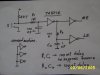
") I'll let you know how it works out!
I'll let you know how it works out!