javman1986
New Member
Hi there,
'm looking for some help regarding a SEPIC circuit design. Basically the idea is to convert from 40V-60V in the input to 100V in the output (1% ripple). The load can vary between 10W and 20 W. Switching frequency is 50 KHz and operation is CCM. I am not too familiar with power electronics nor LTSpice so I am having some troubles.
The circuit I used for the design is the following:

What I attempted to do:
a) Calculate the range for the duty ratio:
[latex]\frac{Vo}{Vin}=\frac{100}{40}=\frac{D}{1-D} [/latex]
and the same for 60V, so I obtained D between 0.625 and 0.714.
b) For the capacitor C2 chose it to be 10u,
c) Output current and load:
[latex] Io=\frac{Pmax}{Vo}=\frac{20W}{100V}=0.2A [/latex]
d) Current ripple in the inductors (peak-to-peak = 40% of max. input current):
[latex] \Delta I_{l}=I_{in}\times 0.4=Io \frac{Vo}{Vin_{min}}=0.2A\times\frac{100V}{40V}\times0.4=0.2A [/latex]
e) Inductances
[latex] L1=L2=\frac{Vin_{min}\times Dmax}{\Delta I_{l}\times f_{s}}=\frac{40V\times0.714}{0.2A\times50KHz}=2.856 mH [/latex]
f) MOSFET
Vds < Vin+Vo
I chose IRF640 (Vds=200V)
g) Diode to be 1N4003
h) Output capacitor
[latex] C_{out}\geq\frac{Io\times D_{max}}{V_{ripple}\times0.5\times f_{s}}=\frac{0.2A\times0.714}{0.01\times100V\times0.5\times 50KHz}=5.712uF [/latex]
I chose 27 uF
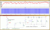
My circuit in LTSpice:

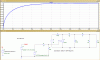
I am getting a warning saying the definition of SW cannot be found, but the simulation seems to run fine. However, the results are totally wrong as the output voltage seems to blow up. This is what I'm getting for Vin=60V (D=0.625):

Also with Vin=40V (D=0.714), the Vo is not the same than in the 60V case. I would appreciate your help giving me some advice on what I could be doing wrong.
Changing the values of the inductances, I got them wrong; the result is still wrong though.
Regards
'm looking for some help regarding a SEPIC circuit design. Basically the idea is to convert from 40V-60V in the input to 100V in the output (1% ripple). The load can vary between 10W and 20 W. Switching frequency is 50 KHz and operation is CCM. I am not too familiar with power electronics nor LTSpice so I am having some troubles.
The circuit I used for the design is the following:
What I attempted to do:
a) Calculate the range for the duty ratio:
[latex]\frac{Vo}{Vin}=\frac{100}{40}=\frac{D}{1-D} [/latex]
and the same for 60V, so I obtained D between 0.625 and 0.714.
b) For the capacitor C2 chose it to be 10u,
c) Output current and load:
[latex] Io=\frac{Pmax}{Vo}=\frac{20W}{100V}=0.2A [/latex]
d) Current ripple in the inductors (peak-to-peak = 40% of max. input current):
[latex] \Delta I_{l}=I_{in}\times 0.4=Io \frac{Vo}{Vin_{min}}=0.2A\times\frac{100V}{40V}\times0.4=0.2A [/latex]
e) Inductances
[latex] L1=L2=\frac{Vin_{min}\times Dmax}{\Delta I_{l}\times f_{s}}=\frac{40V\times0.714}{0.2A\times50KHz}=2.856 mH [/latex]
f) MOSFET
Vds < Vin+Vo
I chose IRF640 (Vds=200V)
g) Diode to be 1N4003
h) Output capacitor
[latex] C_{out}\geq\frac{Io\times D_{max}}{V_{ripple}\times0.5\times f_{s}}=\frac{0.2A\times0.714}{0.01\times100V\times0.5\times 50KHz}=5.712uF [/latex]
I chose 27 uF
My circuit in LTSpice:
I am getting a warning saying the definition of SW cannot be found, but the simulation seems to run fine. However, the results are totally wrong as the output voltage seems to blow up. This is what I'm getting for Vin=60V (D=0.625):
Also with Vin=40V (D=0.714), the Vo is not the same than in the 60V case. I would appreciate your help giving me some advice on what I could be doing wrong.
Changing the values of the inductances, I got them wrong; the result is still wrong though.
Regards
Attachments
Last edited: