Continue to Site

Welcome to our site!

Electro Tech is an online community (with over 170,000 members) who enjoy talking about and building electronic circuits, projects and gadgets. To participate you need to register. Registration is free. Click here to register now.

  • Welcome to our site! Electro Tech is an online community (with over 170,000 members) who enjoy talking about and building electronic circuits, projects and gadgets. To participate you need to register. Registration is free. Click here to register now.

Help reading this schematic

Status
Not open for further replies.
Hello
I would like some help reading the following:
schem1.jpg

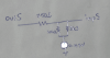
Here you can see an Output digital signal and an input signal (which is analog)
Now I can see a voltage divider (I suppose 100 means 100Ω...what do you think?) therefore the voltage there would be (100/(3400))*5V= 0.147V ...
But how about the rest (from OutS to the point where it reaches the voltage divider) ?? How does this work and what does this mean?

My first question is to understand the parts in black. Additionally can someone explain me what I think is a zener diode there (in blue)? But the main thing I want to understand is the black part

thanks a lot
 
Yes, 100 would mean 100 ohms.
Your voltage divider calc (neglecting the 750 ohm resistor) is correct.
To work out the voltage at inpS, taking into account the 750 resistor, simply change the divider you already calculated for into its Thevenin equivalent (i.e. a resistor to 0.147V; the resistance will be the equivalent parallel resistance of 3.3K and 100). You should then be able to work it out from there.
The zener is possibly to clamp the outS voltage to a safe level
 
What Dougy said is right if "outS" is 0 and +5V.
We don't really know that. Maybe it is 0V and 6.8V (the diode voltage). Maybe it is some quite strange. Probably 0 and +5.
 
Well the left part is a ATTiny2313 so I think it is 5V. With 5V I think I understood the method

However if the levels are 0 and 3.3V it becomes a little messier, doesn't it?
 
What Dougy said is right if "outS" is 0 and +5V.
We don't really know that. Maybe it is 0V and 6.8V (the diode voltage). Maybe it is some quite strange. Probably 0 and +5.
the range of outS doesn't affect how the divider works.
 

Attachments

  • div.png
    div.png
    36.6 KB · Views: 145
Like Dougy & Ron I assumed we were looking at analog signals. What it the circuit meant to achieve ? I have just checked the data sheet on the ATtiny 4313 and it does not have any analog outputs. Also what is the deveice on the right ? If we assume a logic low is zero volts and a logic high is 5.0 volts and the output resistance of the ATtiny 4313 is zero ohms (A very big assumption).
In case you do not understand Thevenin & Nortons theorems I will do the calculation for the 0 and 5 volt situation without using Thevenims theorem. (Thevenims theorem makes that calculation much simpler if the output of the left hand part was 3.3 volts)
When the the output is low (0 volts) We have a potential divider with 100 ohms in parallel with 750 ohms ( 88.24 ohms.) to 0 volts and a 3.3K to 5 volts so the voltage at the output is (88.24/3388.24) x 5 = 0.1302 volts. When the output is at 5 volts we have a potential divider with a 750 ohm in parallel with a 3.3k (611.1 ohms.) to 5 volts and a 100 ohm to 0 volts so the voltage output is (100/711.1) x 5 = 0.703 volts.

Les.
 
So it's a level shifter with input protection, possibly feeding into an open base?
 
Thanks for your post.
Well, as I wrote in the first post OutS is digital. I am assuming it is 0-5V. (Havent checked the ATtiny datasheet).
Thank you too for your calculation. It makes a lot of sense!.
Since now I am using 3.3V micros I am also interested in see what this circuit would mean in that case but in that case I wouldnt be able to just apply parallelism right? as I said kind of messy.

About the circuit, I dont think it is a circuit I am going to implement but I found this in a schematic using a part I am going to use. The right side is a stepper controller, the SLA 7052M and the pin is the Ref pin. In the datasheet they use a voltage divider and a transistor as switch but here I found an implementation without transistors, just as I posted in the first post and I wanted to understand what does the schematic was trying to achieve.

As for me I am going to use a SLA7084 but the circuit I am planning is way simpler ...

EDIT: I am wondering what the guy who did this schematic was trying to do...
ideally the thing that is suggested in the datasheet is two Voltages in inpS of 0.7V and >2V. In 0.7V the motor runs and in >2V the motor is off...
But with the voltages calculated (0.7 and 0.1) this does not happen...mmmmm strange...


Like Dougy & Ron I assumed we were looking at analog signals. What it the circuit meant to achieve ? I have just checked the data sheet on the ATtiny 4313 and it does not have any analog outputs. Also what is the deveice on the right ? If we assume a logic low is zero volts and a logic high is 5.0 volts and the output resistance of the ATtiny 4313 is zero ohms (A very big assumption).
In case you do not understand Thevenin & Nortons theorems I will do the calculation for the 0 and 5 volt situation without using Thevenims theorem. (Thevenims theorem makes that calculation much simpler if the output of the left hand part was 3.3 volts)
When the the output is low (0 volts) We have a potential divider with 100 ohms in parallel with 750 ohms ( 88.24 ohms.) to 0 volts and a 3.3K to 5 volts so the voltage at the output is (88.24/3388.24) x 5 = 0.1302 volts. When the output is at 5 volts we have a potential divider with a 750 ohm in parallel with a 3.3k (611.1 ohms.) to 5 volts and a 100 ohm to 0 volts so the voltage output is (100/711.1) x 5 = 0.703 volts.

Les.
 
Last edited:
Since now I am using 3.3V micros I am also interested in see what this circuit would mean in that case but in that case I wouldnt be able to just apply parallelism right? as I said kind of messy.
Based on the circuit I posted above (Thevenin equiv.), the inpS can be calculated for any outS:

CodeCogsEqn.gif
 
Yes, it looks like a typo. Voltage divider equation should be as you have stated it
 
Status
Not open for further replies.

Latest threads

New Articles From Microcontroller Tips

Back
Top