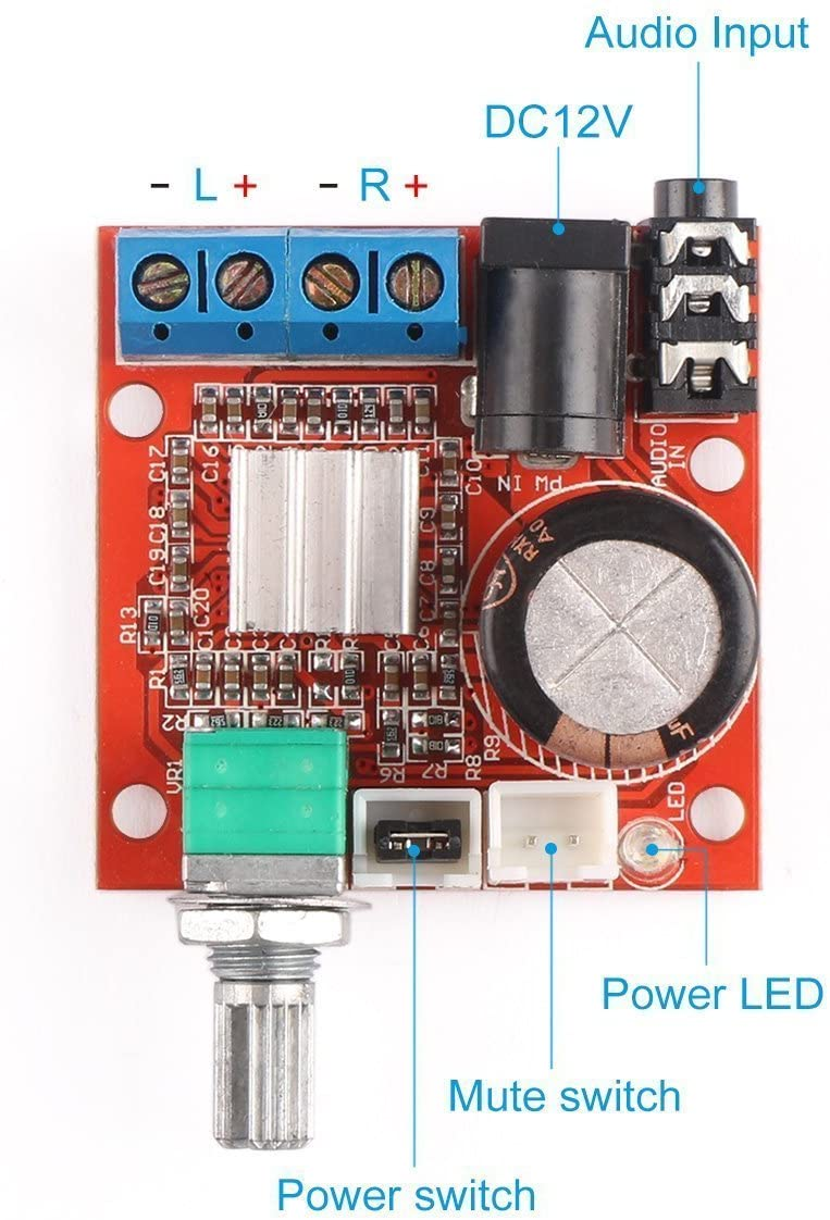
I'm trying to add an off switch to my amp. The board has a jumper described as "Power switch":

And another described as "Mute".
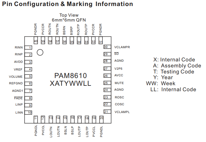
But the datasheet for the PAM 8610 chip has 3 pins that could conceivably be used to implement either of these two functions:
Pin 25 is almost certainly used to provide the "Mute switch" jumper on the board, but which of the other two is used for the power switch is less clear?
The datasheet also carries this information:
High level input voltage: SD... 2.0V to Vdd. MUTE, FADE ... 2.0V to 5V.
Low-level input voltage: SD ... 0 to 0.3V. MUTE, FADE ... 0 to 0.3V
Apart from the fact that the jumpers are only single position, which I think means they are left floating rather pulled down when left open; there is the difference in the max input voltage.
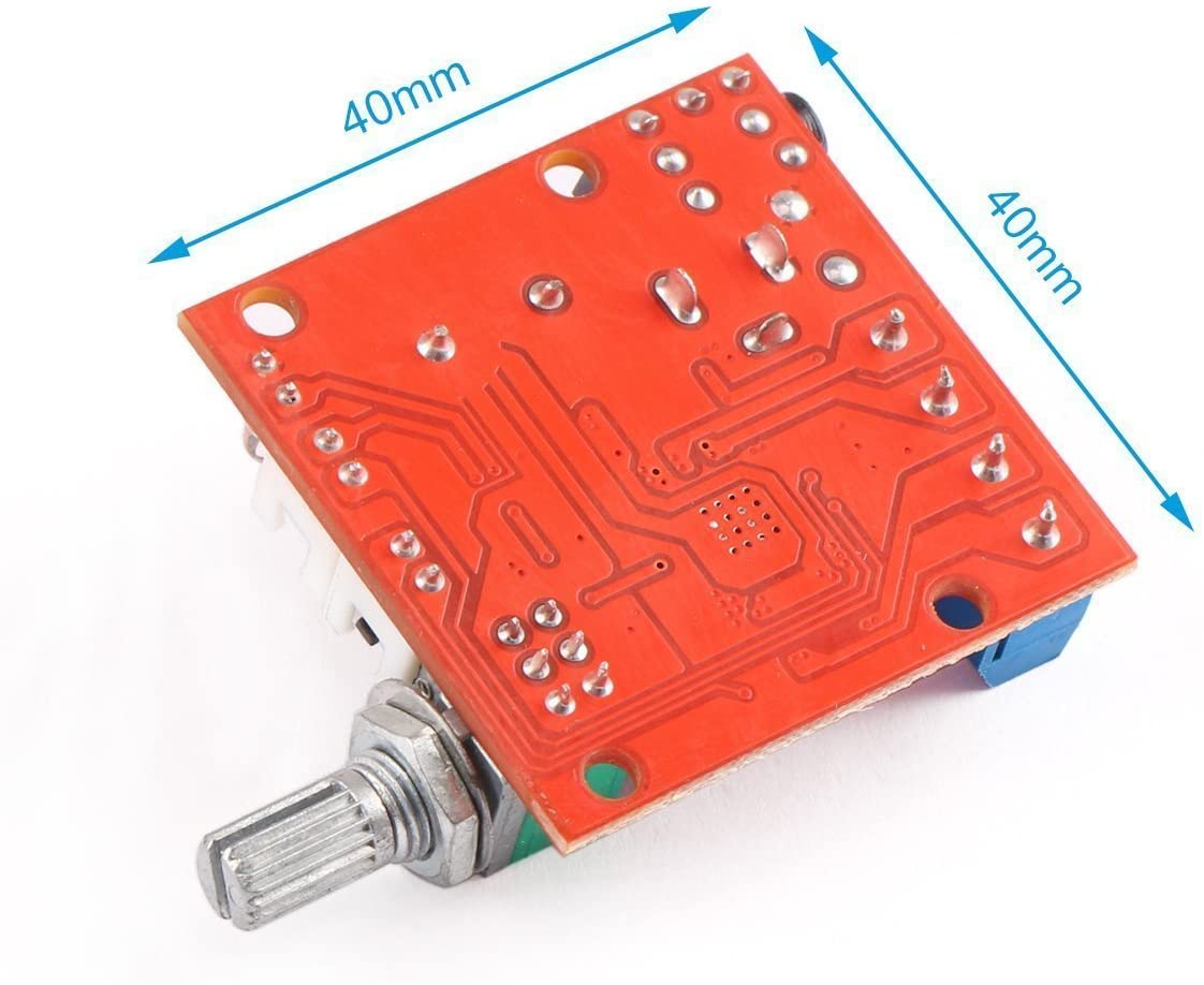
I have a DPDT push switch I intend to use (one pole of) as the on off switch and was considering tying the pin to ground when off, but the chip has several "grounds"; and there is the problem of working out which of the two jumper pins is connected to the SD or FADE pin on the chip. The 6x6mm chip is completely obscured by a 10x10mm heat sink; and the tracks and vias on the underside don't match up with the physical pin layout shown in the datasheet:


Perhaps I should just use a single throw and forget grounding?
Thoughts?
Cheers, Buk.
And another described as "Mute".
But the datasheet for the PAM 8610 chip has 3 pins that could conceivably be used to implement either of these two functions:
Code:
8     FADE    Input for controlling volume ramp rate when cycling SD or during power-up.
                      A logic low on this pin places the amplifier in fade mode. A logic high on
                      this pin allows a quick transition to the desired volume setting.

25     MUTE   A logic high on this pin disables the outputs and a logic low enables the outputs

29    SD        Shutdown signal for IC (low= shutdown, high =operational).
                      TTL logic levels with compliance to VCC.
Pin 25 is almost certainly used to provide the "Mute switch" jumper on the board, but which of the other two is used for the power switch is less clear?
The datasheet also carries this information:
High level input voltage: SD... 2.0V to Vdd. MUTE, FADE ... 2.0V to 5V.
Low-level input voltage: SD ... 0 to 0.3V. MUTE, FADE ... 0 to 0.3V
Apart from the fact that the jumpers are only single position, which I think means they are left floating rather pulled down when left open; there is the difference in the max input voltage.
I have a DPDT push switch I intend to use (one pole of) as the on off switch and was considering tying the pin to ground when off, but the chip has several "grounds"; and there is the problem of working out which of the two jumper pins is connected to the SD or FADE pin on the chip. The 6x6mm chip is completely obscured by a 10x10mm heat sink; and the tracks and vias on the underside don't match up with the physical pin layout shown in the datasheet:
Perhaps I should just use a single throw and forget grounding?
Thoughts?
Cheers, Buk.
