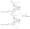
You're using the two devices in completely different modes - the bottom FET is common source, so is a digital switch - either ON or OFF. But your top FET is common drain, so works as an analogue amplifier, and will get very hot. I've not checked the spec. of the devices, but presumably the previously mentioned 6V is what it takes to turn the FET fully ON? - so with the gate at 12V the source will still be at 6V, because it has to be 6V lower than the gate.
The bottom transistor feeds 12V to the gate, and the source is 12V lower, so it's switched ON nice and fully.
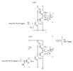
It's exactly the same with both FET's and bi-polar, for switching you want the load to be in the drain/collector, not the source/emitter.
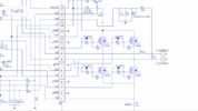
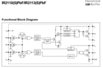
The IR2110 (Like the IR2112 I mentioned previously) has boot-strapping, so allows the top FET to turn ON fully, by creating more than 12V to feed the top FET gate. It's fully explained in the datasheet and application notes.
So either use a boot-strapped driver IC, or change the top FET to P-type.