Continue to Site

Welcome to our site!

Electro Tech is an online community (with over 170,000 members) who enjoy talking about and building electronic circuits, projects and gadgets. To participate you need to register. Registration is free. Click here to register now.

  • Welcome to our site! Electro Tech is an online community (with over 170,000 members) who enjoy talking about and building electronic circuits, projects and gadgets. To participate you need to register. Registration is free. Click here to register now.

H-bridge discrete components: non-oscillation issue

Status
Not open for further replies.

earckens

Member
An H-bridge with discrete components (mosfets) did work in a prototype board, then also in a manufacured PCB, and in a another PCB version (same layout for the bridge) it refuses to oscillate. Difference with the new PCB is a slightly further positioning of Q17 (13mm). Tracks measured and ok, signals arrive at Q17 and its drain. When only using Q19 and Q18 oscillation is ok, when Q21 and Q20 inserted, no oscillation and high current draw. I make sure the 12V is applied only a second or so to avoid blowing the mosfets.
Source is a 555 timer with approx. 10Hz output.
I replaced the mosfets, still the same.
The trigger signal is 12V pp.
What could be wrong?

test.png
 
Measured at Q18, right after start-up (yellow marker above left shows trigger instance): blue = gate, yellow = drain
EDIT: this is N-channel, so why is drain not low (conducting) when gate is high?
upload_2018-7-17_12-16-54.jpeg
 
The circuit cannot work as drawn.
The top power FETS are show as if their internal diodes are always forward biassed and conducting.

Were they fitted reversed or a different type in the original boards?


Personally, I'd never rely on a cross-connected drive like that, or use anything that relies on opposite polarity devices with shared drive signals - you are at the total mercy of production tolerances & random component changes.

For production reliability you should really have drive signals that will operate regardless of supply and device tolerances.

eg. In a very similar circuit, we have two small N channel FETs, with gates driven from the same signals as the lower bridge FETs and and driving the opposite top FET of the bridge.
It's immune to voltage variations over a wide range and as long as you do not drive both inputs at the same time, it's immune to any pass-through current effects.

For a simple drive for that, you could use eg. a 4017 with four outputs diode connected to one input, a gap, then the next four to the other input. That gives a basic non-overlap drive signal.
 
Last edited:
The circuit cannot work as drawn.
The top power FETS are show as if their internal diodes are always forward biassed and conducting.

Were they fitted reversed or a different type in the original boards?
You are spot-on!!!

In the original schematic (the previous pcb, I just checked) they were correct, when drawing the new schematic I took the same components but screwed up with drain and source positioning of the P-channels.

Thanks!!
 
The circuit cannot work as drawn.
(...)

Personally, I'd never rely on a cross-connected drive like that, or use anything that relies on opposite polarity devices with shared drive signals - you are at the total mercy of production tolerances & random component changes.

For production reliability you should really have drive signals that will operate regardless of supply and device tolerances.

eg. In a very similar circuit, we have two small N channel FETs, with gates driven from the same signals as the lower bridge FETs and and driving the opposite top FET of the bridge.
It's immune to voltage variations over a wide range and as long as you do not drive both inputs at the same time, it's immune to any pass-through current effects.

For a simple drive for that, you could use eg. a 4017 with four outputs diode connected to one input, a gap, then the next four to the other input. That gives a basic non-overlap drive signal.
Can you show a 4017 circuit like that plse?
 
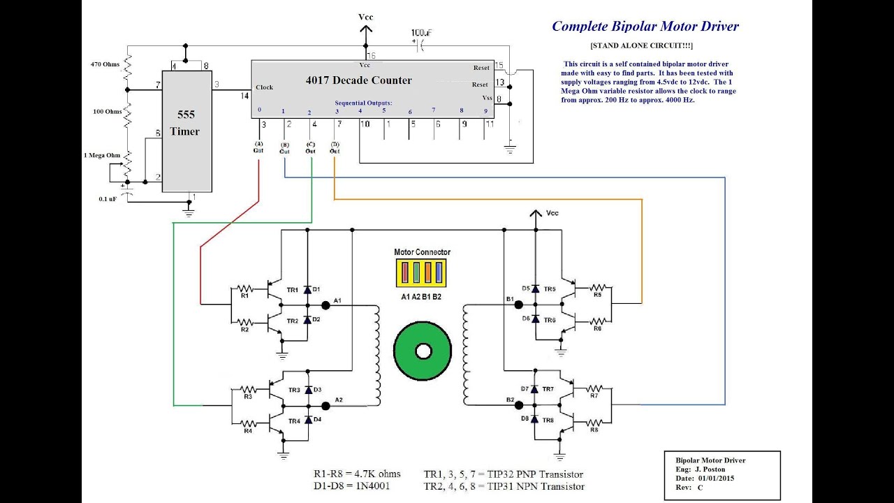
I was thinking of using eg. output 0-3 for one phase and 5-8 for the other, with each block of outputs combined by diode-OR'ing them to give two signals each with 40% duty cycle.
Run the input clock at 10x the required bridge frequency.

Our module was designed to run a specific type of 12V AC air pump motor in a battery operated device and that works very well with 25% duty on each half, using outputs from a different counter and logic setup. If you are using it for anything visual that is probably too low a duty cycle, so I was trying to think of an alternate simple non-overlap drive with a somewhat better duty & the 4017 was the first thing I thought of.

See the photo for the power end of the board [it's a proprietary design & I can't give the whole thing away].
bridge.jpg
The RPs are SIL resistor packs, four separate resistors with the same value in each. We use them a lot in boards we make, it saves a lot of assembly time compared to discrete resistors and makes the overall boards more compact.

The bridge power transistors are D-Pak types and the extra drivers the TO-92 ones. The little bridge rec is to improve flyback energy recovery, rather than relying on diodes in the FETs.


In another device we use a couple of cross-connected schmitt trigger NAND gates with r-c networks to give two outputs from an on-off signal, with a very short but definable non-overlap delay between them. That's designed to drive opposed solenoid coils and only has single ended outputs, but with a delay to allow the field in each coil to decay somewhat before energising the opposite side.

That type of circuit could be used to give an imperceptible all-off delay, but the end use of the design is the main consideration - is going full brick-outhouse, belt-and-braces with everything needed or useful in a particular application?

We pretty much alway do, but it's down to the specific business field and end user cost vs quality requirements.


ps. The stepper circuit above contains exactly the type of design feature I avoid - two opposed transistors sharing a drive signal.
If the drive malfunctions both transistors in each pair turn on at the same time...
It's a "cheap and cheerful" method but not failsafe.
 
Last edited:
Status
Not open for further replies.

Latest threads

New Articles From Microcontroller Tips

Back
Top