Continue to Site

Welcome to our site!

Electro Tech is an online community (with over 170,000 members) who enjoy talking about and building electronic circuits, projects and gadgets. To participate you need to register. Registration is free. Click here to register now.

  • Welcome to our site! Electro Tech is an online community (with over 170,000 members) who enjoy talking about and building electronic circuits, projects and gadgets. To participate you need to register. Registration is free. Click here to register now.

First time transcribing schematic to a stripboard and would appreciate verification that I've done so correctly.

Status
Not open for further replies.

The_Schnebbz

New Member
Greetings all,

I'm currently attempting to build a microphone in the same style as [Scott Helmke's "Alice"] mic. Following the parts list and schematic that they've posted to their website.
Given that this is the first electronics DIY project I'm attempting (the wisdom of using this as a first project is yet to be seen.) I'd appreciate anyone looking over how I've translated from the schematic to a stripboard to make sure I haven't made any silly mistakes. (And of course any applicable advice is welcome as well.)

The schematic I worked from (from Scott Helmke's website)
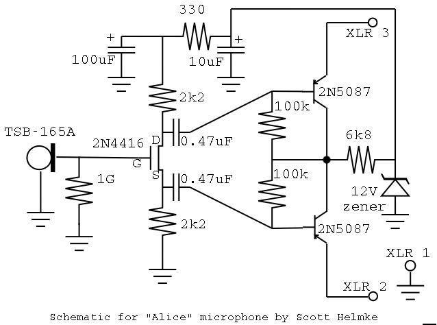
alice-schematic.jpg


And how I laid the above out in DIYLC
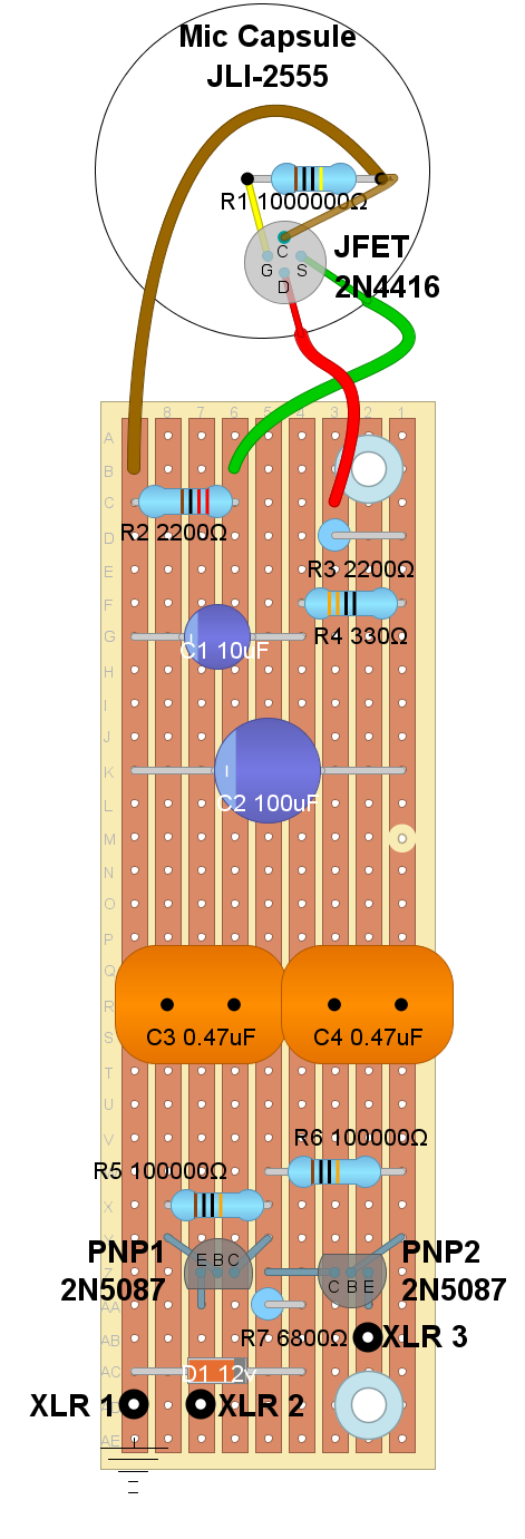
Alice Mic forum version.png


(If it makes a meaningful difference, Mouser was out of specifically the 2N4416 JFETs at the time, so the one I actually have on hand is the 2N4416A variant. Here's a [Link] to the datasheet from Mouser, the difference I'm seeing is the breakdown voltage is -30v for the 2N4416 and -35v for the 2N4416A. I'm not sure how or if that will effect the rest of the circuit.)

Apologies in advance for committing any of the common newbie mistakes. I've undoubtedly got several unknown-unknowns related to the topic of DIY circuits, so if there's something that could be changed to improve readability or if there's just something that looks odd, feel free to let me know and I'll do my best to fix it!

Thanks!
 
One check I do with Vero (strip) board is to run a box-cutter down between all the tracks, it automatically detects and usually removes hair line solder bridge that may be present but not evidently visible.
Also a minor point, the power-common symbol should normally be used, not the Earth GND version.


1661015259099.png
 

Attachments

  • 1661013929631.png
    1661013929631.png
    6 KB · Views: 183
Last edited:
One check I do with Vero (strip) board is to run a box-cutter down between all the tracks, it automatically detects and usually removes hair line solder bridge that may be present but not evidently visible.
Also a minor point, the power-common symbol should normally be used, not the Earth GND version.

<snip>
Thanks! The tip with the box cutter will definitely be useful, and also thanks for pointing out the difference between the earth ground and common ground symbols.
 
The FET gate resistor is supposed to be one Gigaohm; 1000 Megaohms.
You are showing a 100K there? That will not work, if you are actually using that?
 
On Veroboard / stripboard I've found it best to put the radial components on their natural lead spacing.

You seem to have done that on the non-polarised 0.47 μF capacitors, but not on the electrolytic capacitors. I think that you will find that the electrolytic capacitors will be rather wobbly if fitted as you show them.

The transistors leads are closer together than the holes on the board, so the leads have to be spread a bit, but I wouldn't spread them as much as you have.

I have almost always needed to used a few wire links on Veroboard / stripboard projects.

The components should be on the side of the board that does not have the copper on it.
Thanks for the advice! The non-polarized capacitors are actually one track narrower than their natural spacing, although on a test fit even with their natural spacing they're too tall for the planned case (a 1" diameter copper pipe.) So either way they'll need to be laid down (which is why they have the vertical free space that they do in the diagram.)
My initial attempt at a layout did have the thought process of minimizing jumper wires and trace cuts, but we'll see if I can make things a bit better with not stretching the leads so much.

On previous internet searching for general tips and tricks of laying out components on a veroboard I did see the point made that the parts go on the opposite side of the copper traces, so you're at least not the first to have to mention it. =p
It's good to repeat it though for anyone else that may happen to stumble upon this.

I had noticed that but thought the OP displayed it as though looking through the board?.
Like the Stripboard layout software pgm's do.
I wasn't sure if the OP was intending to put the components on the copper side or not.
I'd be lying if I said anything beyond "that's what it looks like by default when you make a veroboard in DIYLC (DIY Layout Creator.) If I had to make a guess, I'd say it's something like what MaxHeadRoom said, looking through to the back of the board so that you can visually track the traces going back and forth. Otherwise it'd just look like a flat color plane and wouldn't be much more useful than just putting the components on a grid.

No worries, the components will go on the no-copper side, the leads poke through and get soldered onto the yes-copper side. =p


For better or worse, my attempt to reduce how much the leads on the electrolytic capacitors and transistors have to stretch:
Alice Mic forum version V3.png


If anything, I'm happy that the discussion seems to be more towards "Things would be more optimal this way" and "Make sure you don't hit this pitfall that can be easy for someone new to miss," than "This component is in completely the wrong spot and will recreate an ElectroBoom video if it gets plugged in."
 
Re Schematics, as per the OP.
One tip, if you intend getting in to drawing schematics etc, is to use a 'dot' at every junction points, as is done only once at the junction of the collectors of the schematic in the OP.
It should be at every junction.
One excellent free S/W for schematics/boards etc, is Kicad.
 
I'd not get too hung up on physical layout - if everything fits & connects correctly, just go for it!

These are roughly similar things - the small board is an in-line adapter from a Shure three terminal electret capsule mic to XLR, a device I made a batch of for whole house home automation mics a couple of decades ago, before I'd heard of Schoeps etc.

They are similar to the circuit you posted, but with the mic capsule functionally in place of the FET - however they use NPN output device arranged as modulated current sources, which I still prefer. (Metal can BC107B's, in those).

The long thin one is a similar output section plus phase splitter & power filtering, shoehorned dead-bug style into the 16mm diameter bodies of a pair of rather nice old electret mics I've had since the 70s.

They originally had an AA battery in series with the audio out, which I always thought was a somewhat vile arrangement. I made two of those "boards"? to convert them to XLR compatible a couple of years ago.

IMG_7572.jpg


IMG_7573.jpg
 
Re Schematics, as per the OP.
One tip, if you intend getting in to drawing schematics etc, is to use a 'dot' at every junction points, as is done only once at the junction of the collectors of the schematic in the OP.
It should be at every junction.
One excellent free S/W for schematics/boards etc, is Kicad.
I'd be surprised if I get much into the drawing part of schematics, but who knows what will happen in the future. I'll file that info under "things I know", thanks.
Kicad is another name I saw when looking for software to use, I'll keep it in mind if DIYLC isn't able to do what I need.

I'd not get too hung up on physical layout - if everything fits & connects correctly, just go for it!

These are roughly similar things - the small board is an in-line adapter from a Shure three terminal electret capsule mic to XLR, a device I made a batch of for whole house home automation mics a couple of decades ago, before I'd heard of Schoeps etc.

They are similar to the circuit you posted, but with the mic capsule functionally in place of the FET - however they use NPN output device arranged as modulated current sources, which I still prefer. (Metal can BC107B's, in those).

The long thin one is a similar output section plus phase splitter & power filtering, shoehorned dead-bug style into the 16mm diameter bodies of a pair of rather nice old electret mics I've had since the 70s.

They originally had an AA battery in series with the audio out, which I always thought was a somewhat vile arrangement. I made two of those "boards"? to convert them to XLR compatible a couple of years ago.

<snip x2>

Thanks! And yeah, probably time to just go at it, if everything goes well then great; if not then troubleshooting will just be part of the fun. lol

Those look neat (at least to me) the 16mm diameter case especially looks like it'd be a challenge to work with.
A battery in series with the audio out kind of reminds me of those ethernet powerline adapters that use your homes electrical wiring to transmit data without having to run actual network cables. =p
 
Status
Not open for further replies.

Latest threads

New Articles From Microcontroller Tips

Back
Top