Continue to Site

Welcome to our site!

Electro Tech is an online community (with over 170,000 members) who enjoy talking about and building electronic circuits, projects and gadgets. To participate you need to register. Registration is free. Click here to register now.

  • Welcome to our site! Electro Tech is an online community (with over 170,000 members) who enjoy talking about and building electronic circuits, projects and gadgets. To participate you need to register. Registration is free. Click here to register now.

First attempt at designing a low input voltage boost converter

Status
Not open for further replies.

Gasboss775

Member
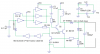
I wanted to have a go at designing a boost converter that could power say a 9volt circuit from 2 x NiMH cells. The circuit works quite well in fact with as much as 85% efficiency. My problem is that at certain combinations of input voltage and / or load it becomes unstable with the output voltage cycling up and down over about a 300mV range. R5 & C3 were a crude attempt at compensation ( a subject that I can't really claim to understand very well ) from the little I do know I suspect that the problem is related to compensation or lack there of.
 

Attachments

  • Low Voltage Boost Converter.png
    Low Voltage Boost Converter.png
    44.5 KB · Views: 461
The problem may be due to insufficient base current in Q2, since the TLC555 is rated to source only 20mA.
 
I decided to go about it in a slightly different way. Used a CD40106 hex Schmitt inverter as a gated oscillator driving the switching transistor via a bc549c ( hFE > 500 ) the idea of putting a Schmitt trigger between the feedback transistor and the oscillator was to ensure clean gating. It was able to supply greater current than the previous circuit so there probably was a problem with insufficient drive from the CMOS 555.
 

Attachments

  • 40106 Stepup converter 3 v to 9v5.png
    40106 Stepup converter 3 v to 9v5.png
    60.5 KB · Views: 306
I decided to go about it in a slightly different way. Used a CD40106 hex Schmitt inverter as a gated oscillator driving the switching transistor via a bc549c ( hFE > 500 ) the idea of putting a Schmitt trigger between the feedback transistor and the oscillator was to ensure clean gating. It was able to supply greater current than the previous circuit so there probably was a problem with insufficient drive from the CMOS 555.
The problem may have been using the reset pin for the feedback. The first pulse from a 555 after a reset is longer than normal so may upset the circuit.
Often the control voltage pin is used instead.
 
The problem may have been using the reset pin for the feedback. The first pulse from a 555 after a reset is longer than normal so may upset the circuit.
Often the control voltage pin is used instead.

Yeah I've seen the feedback taken to pin 5. I was working on the premise that the feedback would regulate by gating the oscillator rather than adjusting duty cycle or frequency. I have achieved some success with this approach in my second circuit ( post #4 on this thread ) using a hex Schmitt input inverter ( CD40106, though 74HC14 could work too, I think )

I forgot to mention the circuit in post #4 can operate down to < 2 volts albeit with reduced output voltage and poorer regulation. My intention is to use 3 NiMH batteries, which fall to around 0.9 volts at the end of their discharge cycle ( hence 2.7 volts for three cells ) I think using 2 cells ( 1.8 volts at end of discharge cycle ) would be cutting it a bit close!

I haven't quite decided what to use the circuit for yet, the motivation was purely the intellectual challenge. I had thought that with 5 volts output it could be used to power USB devices though might need to make adjustments to allow for greater output current.
 
Last edited:
In the post #4 circuit the collector of Q2 shouldn't go directly to Vcc. As shown, Q1 and Q2 virtually short the supply.
You might want to add suppression components across the inductor to prevent back-emf voltage spikes frying Q1.
 
In the post #4 circuit the collector of Q2 shouldn't go directly to Vcc. As shown, Q1 and Q2 virtually short the supply.
You might want to add suppression components across the inductor to prevent back-emf voltage spikes frying Q1.

Yeah, that occurred to me too when I was looking at the schematic again, I was thinking about adding a resistor between Q1 emitter and Q2 base. What values of R & C would you recommend as a snubber circuit?
 
The suppression components would depend on the peak inductor current, Q1 characteristics (I don't have a Spice simulation model for a BD139) and switching frequency.
 
The suppression components would depend on the peak inductor current, Q1 characteristics (I don't have a Spice simulation model for a BD139) and switching frequency.

Could you suggest ballpark figures? I have spare transistors so can afford to muck up by trial and error! The switching frequency varies due to the action of the regulation.
 
Another possibility is a high voltage power transistor. I have 4 BUL128A, these are rated at Vceo = 400V and are suitable for inductive loads, the only downside is that hFE is very low, will either need to drive with a Darlington or a low power MOSFET like a 2n7000.
 
Another possibility is a high voltage power transistor. I have 4 BUL128A, these are rated at Vceo = 400V and are suitable for inductive loads, the only downside is that hFE is very low, will either need to drive with a Darlington or a low power MOSFET like a 2n7000.

Didn't work well due to very low hFE of switching transistor.

Turns out that replacing the whole lot with an IRL2910 driven directly from the 40106 works best. More efficient, no stability problems so far, though I haven't tested thoroughly.
 
Do you have any power MOSFETs available? The 555 should drive one of them without any problems. There are a number of boost converter circuits floating around, using a 555 and a MOSFET that work quite well.
 
For spike limiting I'd try a zener diode in series with a normal silicon diode. The zener voltage would be ~75% of the rated max collector voltage of the transistor, so ~60V for a BD139.
 
For spike limiting I'd try a zener diode in series with a normal silicon diode. The zener voltage would be ~75% of the rated max collector voltage of the transistor, so ~60V for a BD139.

Thanks again for your help. I am using an IRL2910 MOSFET now as the switch, max drain source voltage is 100v, but looking at the waveform at the junction of the drain and inductor on my 'scope it appears that the 1n5822 is effectively clamping the drain at just above the output voltage. I've built a number of stepupcircuits over the last 3 months and this seems to have been the case in all of them and the lack of dead transistors seems to support this notion.
 
If the clamping action is reliable then the spike-limiting components are probably a bit of a belt-and-braces luxury.
 
The IRL2910 has an internal diode to deal with spikes

LG
 
Good luck, but I believe the only really effective way to do a boost converter from 2 NIMH up to 9V (?power level) is to use a “Pilot” mini boost converter to give you an “at_least_4V” bias rail which can be used to power the main boost pwm controller.
Two nimh’s in series will go down to <2V quite quickly, and few controllers can be powered from that……apart from some of the mini boost converter IC’s which they have on ti.com or linear.com…so the idea is to use one of them to give you a bias rail

If you use just one controller, then it wont be able to drive the switching transistor with enough Vgs voltage. (specially with the battery voltage dropping as it discharges)
Not only that, but remember that your effective Vin is the battery voltage, minus the esr voltage drop in the inductor, and also minus the esr voltage drop of the fet, and minus the voltage drop in the wiring resistance.
So I would use one of the monolithic mini boost controllers on linear.com or ti.com or intersil.com etc, and that will at least give you a decent voltage bias rail to drive the main boost controller with.
(On another note, I hope the Forth Road Bridge is back open, I got stuck in Rosyth recently, the bridge closed the day after I went over it.)
 
...Another point is that you cannot do current mode control because you have no source sense resistor……this is generally a bad idea, even for voltage mode control….and in fact , any type of control, but I suppose your vin is so low that your not going to get runaway input current ...but it doesmean that you are limited to voltage mode control if you want the control to be smooth...then again, if you are prepared to not have a smooth train of switching pulses then you wont care about that......indeed your cout is so high that any non smooth pulsing isn't likely to show up in the output voltage , as long as your pout is not too high.

Of course, another point is that you probably couldn't have a source sense resistor anyway as it would drop too much of your precious v(in).

So if you want smooth control with no sense resistor, then you are limited to voltage mode control, with all the problems that that may gave with respect to oscillation between the boost inductor and the output capacitor....unless properly compensated.
If its just low power then simple on/off control is fine. Another form of control that you cannot do without a low side sense resistor is constant-off-time control.
But again, should you care...maybe not.
if YOU REDUCE THE SIZE OF YOUR OUTPUt cap then you may get problems with oscillations in vout, if on/off control is used, specially if your switching frequency is near to the LC resonant frequency of the boost inductor and the output cap.
 
Last edited:
Status
Not open for further replies.

Latest threads

Back
Top