Continue to Site

Welcome to our site!

Electro Tech is an online community (with over 170,000 members) who enjoy talking about and building electronic circuits, projects and gadgets. To participate you need to register. Registration is free. Click here to register now.

  • Welcome to our site! Electro Tech is an online community (with over 170,000 members) who enjoy talking about and building electronic circuits, projects and gadgets. To participate you need to register. Registration is free. Click here to register now.

Filter circuit for car ignition coil tach

Status
Not open for further replies.
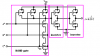
OK, better late than never, I guess. Here's the tardy schematic. Hopefully the two parallel gates will have enough drive for your tach.

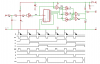
EDIT: Corrected error in schematic and added timing diagram. I drew the duty cycle as 20%, since you mentioned that, but it should work with any duty cycle. Note that, at 33.3Hz, there is a component in the output at 8.3Hz, due to the fact that you are dropping every 4th pulse. You may see jitter in the tach at low RPMs.
 

Attachments

  • tach5 with timing.PNG
    tach5 with timing.PNG
    34.2 KB · Views: 994
Last edited:
Thank you for the diagram. Can you help explain how some of it works for me? I see we now have a 4023 chip in there. A quick search on google says it is a tripple input NAND gate (which I gathered from the symbol on the diagram) but it also says it has a buffered output. I'm not sure what it means if the output is buffered?

Also I'm not sure I understand how that very last 4023 NAND gate will be driven from the 4017 (buffered through the three 4093 gates) as each of the three inputs on that last 4023 will go high one at a time and never all at the same time right?

Thanks again for the help. I will pick up a 4023 and see if I can get this circuit built and tested.

Malcolm
 
MalcolmV8 said:
Thank you for the diagram. Can you help explain how some of it works for me? I see we now have a 4023 chip in there. A quick search on google says it is a tripple input NAND gate (which I gathered from the symbol on the diagram) but it also says it has a buffered output. I'm not sure what it means if the output is buffered?

Also I'm not sure I understand how that very last 4023 NAND gate will be driven from the 4017 (buffered through the three 4093 gates) as each of the three inputs on that last 4023 will go high one at a time and never all at the same time right?

Thanks again for the help. I will pick up a 4023 and see if I can get this circuit built and tested.

Malcolm
See my previous post. I edited the schematic (moved one of the 4023s) and added a timing diagram, so you can (hopefully) see how it works.
A buffered gate just means there are internal inverters following the NAND gate. This allows the output drive strength to be kept relatively high while still keeping the input capacitance low. Also, without the inverters, the output drive strength will vary depending on the logic levels present on the various inputs.
 

Attachments

  • CD4023 sch.PNG
    CD4023 sch.PNG
    9 KB · Views: 607
Status
Not open for further replies.

Latest threads

Back
Top