Continue to Site

Welcome to our site!

Electro Tech is an online community (with over 170,000 members) who enjoy talking about and building electronic circuits, projects and gadgets. To participate you need to register. Registration is free. Click here to register now.

  • Welcome to our site! Electro Tech is an online community (with over 170,000 members) who enjoy talking about and building electronic circuits, projects and gadgets. To participate you need to register. Registration is free. Click here to register now.

Explain how this works?

Status
Not open for further replies.
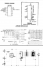
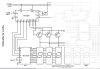
Could someone explain to me how this works from the 4026 to the 7 seg in great detail? I seem to get the drift of all of it especially the clocks and 555 etc but the end output and 4026 driver I lack detail on. How does it drive the 7 seg? what does each pin do? why is each pin conncted their and why? these sort of things..

Truth be told I'm not fond of datasheets when it comes to ICs and they make me go crazy when reading them as I don't tend to retain much from them.


Thank you very much any help is highly appreciated.


some use a 4026 to drive a seg others use a 4511. What are pros/cons of each one?
 
Last edited:
Basically the 4511 converts 4-bit binary to 7 segment, and thats it, it only replaces half of the 4026

that is the second part inside the 4026, the first part of 4026 is a counter circuit that increments on each clock pulse which is not included with the 4511, so using 4511 you would need something more between that and the 555
 
iT'S BEEN 30 YRS SINCE i USED ONE OF THESE CHIPS, so I had to refer to the specs.


Inputs are pins 1,2,3,,15 with V+ = Vdd pin 16 = logic "1" , 0V=Vss pin 8
All the other pins are outputs.

To operate continuously this 7 seg. decoder decade up-counter needs the following.
Clock = 0 to 1 edge
Clock Inhibit=0
Reset=0
Display En IN = 1
Not needed are Ungated "c" segment out and Carry Out signals
the segments are standardized a thru g and LED's usually have a decimal point as well on left or right side.

Edit deleted in Yellow

The segment drivers are active high, so whoever created this schematic made a mistake and used active low segments or "Common Anode" instead of with a a "Common Cathode" which is required with active high out on this driver chip.


upload_2016-4-7_16-52-58.png

Note on the timing chart when RESET is =1 when the OE=1 before the 1st clock all outputs are ON =1 except the centre segment g=0 thus the design you showed won't work. Just need a CC type digit instead.(Common Cathode)
 

Attachments

  • upload_2016-4-7_16-45-7.png
    upload_2016-4-7_16-45-7.png
    592.8 KB · Views: 212
Last edited:
Yes google datasheets for 4510 and 4511, they are both inside the 4026 more or less.
One is a binary counter (well bcd), and the other converts bcd numeric codes into the bit patterns required to display a number on a 7 segment display.
I never really like the 4511, the 6 and 9 are not that clear.
You can cascade more 4026's on that circuit so you can count to 99 or 999, or whatever you want.
 
The 4026 has two basic sections. Referring to the Figure 1 logic diagram on the datasheet (gotta start somewhere), the five flipflops in the upper left corner and the column of 9 NOR gates form a Johnson counter. This is what is inside a 4017. Unlike a binary or BCD counter, a Johnson counter does not make a coded output; it has one individual output line for each count. In fact they cheat a bit on the gating to save some complexity, so there are only 9 gates instead of 10, but it is conceptually the same.

Next up is another gating stack, this time a bunch on inverting-input AND gates. There are 7, one for each segment of the display. If you look at the gate driving segment G, it has 4 inputs. One is the display enable, used to blank the display no matter what the count is. The other three inputs are driven by the counter outputs for numbers 0, 1, and 7. The decoder is using negative logic. Rather than decode when to turn on segment G, it is decoding when to turn it off, probably because this requires fewer gates of inputs. There is no center horizontal segment in the numbers 0, 1, or 7, so this gates turns off the segment for those numbers.

Back to the first paragraph, here's a fun fact: because the segment decoders are decoding when to turns things off rather than on, they do not have to decode the number 8. For an 8, all segments are on, so there is nothing to turn off. This is why the first column of NOR gates has only 9 gates for a 10-output counter. There is no 8 output going into the next section.

Lastly are the output drivers, basically just extra-beefy transistors to handle the LED current. Bright displays can need 20 mA or more per segment, about 10x what a normal CMOS output can drive.

ak
 
The segment drivers are active high, so whoever created this schematic made a mistake and used active low segments or "Common Anode" instead of a "Common (grounded) Cathode" which is required with active high out on this chip.

This part confuses me, you say that its meant to go to ground but it is in the schematic that i have provided, infact it is pretty much the same as the one you have provided unless i'm not seeing something right?

I read your note below the pic but ?
 
Hola John,

Fond or not of datasheets, I found the timing diagrams quite useful to understand precisely...the timing. Once you get used to it, it is going to make your life easier.

Just in case, keep in mind that you could eventually clock those ICs pulse by pulse, provided they are properly debounced.

For any piece of clocked logic, make sure you refer whatever you look at, to the clock's edges. That should help in the understanding. The rest is max/min parameters when you think of using extreme voltages or frequencies (do not go there until you get it working in more "domestic" ranges).
 
I dont know how, but I made a mistake in reading the LED pins
Note the decoder output for zero (0) and outputs "abcdefg" is 1111110 with g being the centre segment as off.
Instead of segment resistors , the design relies on the built-in resistance of old HCxxx CMOS.
74ALxxx CMOS is closer to 50Ω driver resistance, called RdsOn.
upload_2016-4-9_21-0-24.png
 
upload_2016-4-18_21-39-2.png

In this schematic:

1) what is the purpose of the transistors and 4k7 LEDs which connected rom the segment to the 14553.
2) the 1m and 100k resistors which go to ground.
3) 1n capacitor from pin 4 -3

4) I went over the datasheets for the ICs but they were total gibberish to me I understand some concepts but others just fly over my head, If appropriate it would be very nice if someone could explain in great detail how they function in terms of pins and make up etc especially the 14553.
 
This circuit is a simple 3 digit counter with a shared segment bus and time-multiplexed 3 digit display.
Your inputs are; negative edge clock (CP0), Latch enable+ (LE) and Reset. You can LE whenever you want, either while it is counting slowly, or quickly once per fixed interval just before you Reset with repetitive readings like a multimeter at a fixed rate. Meanwhile an internal clock scans each digit fast enough so there is no flicker at say 200Hz to 1kHz, 100Hz will be too slow.
Since you have 3 digits, each ON 1/3 of the time, you must drive it with 3x the average desired current for the same brightness. This can become a challenge to keep the LEDs at display constant brightness for 1 to 7 segments thru the Common side driver.

Digits come in two Common configurations for Anode or Cathode , (CA and CC). The common side is switched on with a constant voltage normally near V+ for CA and near 0V for CC since the Anodes in CA are always positive., and cathodes in CC are always negative to make the diode forward biased.

When using the CMOS counters or decoders, they are usually "positive logic" meaning active high, but the Digit Select outputs are active low on the 14553. The PNP transistors are used as active low current buffers called emitter followers. the emitter current is controlled by the base current * hFE and load. But hFE can vary widely from 50 to 800 , so there are constraints in design to reduce voltage variation for the common side of the LED. Current limiting and brightness is always controlled on the segment side, so the Common side must be a fairly stable voltage..

The 14511B is a BCD to 7 segment latch/decoder/driver whose input comes from the 14553's BCD output below.

upload_2016-4-18_19-5-43.png


The 14553B has a 3−digit BCD counter, a 3 digit latch and a 3 digit MUX with a scanner integrated clock to scan each digit with the correct BCD output during Digit Select. (DS#)
The BCD counters that are cascaded synchronously which means they update from the input clock edge not from preceding outputs, which we call asynchronous counters.
The quad latch at the output of each counter permits storage of any given count. The information is then time division multiplexed, providing one BCD number or digit at a time. Digit select outputs provide display control. Thus one can use a high frequency clock to measure frequency with an accurate Latch Enable interval OR use it to simply count events and always enable thus update the diisplay is as fast as the internal MUX clock in milliseconds.

Brightness control

The 14xxx CMOS types have 300 Ohms internal driver resistance and when all 7 segments are active with say 20mA for large types, each digit might draw up to 140mA thru the transistor, depending on the LED Vf, supply voltage and choice of segment resistor current and any other voltage drops. The transistor must maintain the same voltage out regardless of the number of segments active. Since V output low or VOL is 0V and we consider hFE of 140 for now, then the base current would be 1mA which results in the digit select active low rising to 0.3V with 300 Ohms internal in series. the BC556 cannot handle much more than 140mA without significant voltage drop and the datasheet indicates at 25'C Vbe rises from 0.63 to 0.83V at 140mA. Now the Common Cathodes will be active at 0.3V+0.83=1.1V max and 0+0.63V min. which is a wide range for a 3.6V LiPo cell supply and but they used a 9V source , but perhaps not because using a battery as this current would kill a 9V battery pretty quick.

The given design is not very bright nor very efficient as most of the voltage drop is wasted in resistor heat with approx 12mA/3 average per LED.

It is possible to improve this design to run from a 3.6V LiPo battery which has more current capacity than a 9V alkaline or a standard 5V supply, by choosing more care in selecting the current limiting parts and LED Digit display type.

The Cap across pin 3-4 is a digit scanner clock timer and is explained very well in the data sheet. Like Memory refresh this is a Digit refresh while each digit is driven sequentially. from the latched BCD counter decoder to MUX out.
 
Last edited:
To make accurate current calculations, one needs to know the ESR of each active device to get it's forward voltage drop.
Not easy for rookies.

To do this we consult the spec sheet and look at V vs I and remember that when driving each digit from 0 to 9 there are a minimum of 2 segments with a decimal "1" and 7 segments ON with an "8" since CMOS drivers and emitter followers are not perfect "switches" and each transistor and diode has an equivalent series resistance or ESR.

Note my RED test points for Ohm's Law calculations starts at #0 for Gnd up to #7 for Vbat of ~9V here. The goal is make the common Cathode side constant voltage regardless of number of segments active. Here the transistors T1,T2,T2 need to be binned for very high hFE=500 to allow 1V drop on 4K7's ( too big) for 200 uA = Ib and hope to get 200uA x500 = 100mA to drive each digit and get only 5mA avg. per segment.
upload_2016-4-19_9-19-36.png

----------------------------------------------------------------------------------------------------------------------------------------------------------------------------------------------------------------------------------
Here from the datasheet is another design using the COMMON ANODE with an inverting transistor switch to select each digit with the 14553 internal MUX active low out is inverted to drive each digit in succession with +VDD, while the segments are switched on with active LOW outputs with current limiting resistors.
upload_2016-4-19_9-6-21.png

Its an negative logic output or "active low" BCD to 7 segment 14543 decoder unlike your example with active high out segment drive..

The goal is to have the collector voltage constant for any number of digits ON and thus the current is controlled by the segment R's rather than change brightness depending on the number of digits on. ( poor design). I numbered the test points from 0 to 4 in b lue to show the voltage rise from 0V to Vdd.

10mA avg per segment means 30mA peak with 33% duty cycle.

Note how all the segments LEDs form a parallel bus for 3 digits and a duplicate circuit using Carry Out is need to make a 6 digit counter.
Power FETs make better switches than transistors for this application as they tend to have lower RdsOn than Rce of a bipolar for the same price or size when used as an inverting switch.
Although the schematic looks simple, the calculations for Ohm's law on active devices can get complicated.
Since the transistors must each drive 210mA max and the hFE drops to about 10% when saturated as an inverting switch, we need very high hFE and high current capacity transistors perhaps capable of >=1A.

I already told you `14xxx CMOS is around 300 Ohms ( @5V) actually drops to 200 Ohms at 12V and rises at 3V. Either very special bipolars or better, logic threshold threshold pChannel FET switches ( which weren't invented when these IC's came out in the 70's) . Thus the R's from DS3,DS2,DS1 will be very small values depending on transistor , causing VOL on the DSx outputs to rise due to internal ESR. ( or RdsON if you prefer) THis is OK as long as total power for device is less than absolute maximum worst case of 500mW.
 

Attachments

  • upload_2016-4-19_8-54-35.png
    upload_2016-4-19_8-54-35.png
    119 KB · Views: 153
  • upload_2016-4-19_9-1-47.png
    upload_2016-4-19_9-1-47.png
    119 KB · Views: 235
I'm not going to explain in detail, but I will attempt to answer your questions.
The 4k7's and transistors switch the common cathodes of the display digits to ground, the chip cannot sink enough current by itself so trannys are required.
The 1m and 100k's are pull downs, maybe the designer had long lines to these pins.
The cap from pin 3 to 4 sets the multiplex frequency, this is the rate at which the chip switches from one display digit to the next.
 
John I think 95% of the schematics on the internet are trashy and incomplete, including my postings , because good documentation takes time and pro's cannot release proprietary documents.
So don't be surprised if you can't understand them. But you should be able to or learn to understand the datasheets.

I included part of the BCD counter logic table, and the symbol block with pin-outs. You can see the illustrator did not use the same one.
Notice in the data sheet how inputs are on the left and and outputs on the right and pin numbers are all outside.
But in your ref schema; numerous differences;
  • pin numbers are missing for DS3,2,1
  • CARRY output is on the left going nowhere. ( which is the same as O.F. or overflow and is the /10 clock out used to Carry to next digit stage, if any)
    • Pin 11 is numbered but not labeled on the right , but is actually an INPUT and should be on the left labeled as DIS(able) but grounded as unused.
    • Where chips get more complicated, left/right in/out is not possible such as bi-directional; and large pin count IC's
  • Then we have 3 resistors going nowhere with different values 1M and 100k.
    • I can tell you 1M is OK for local unused terminations but short wires for RESET should be 100K and long wires 10K with an RF cap.
    • You may conclude from that if this is true , the designer wanted to suppress small noise with a lower R value going to a normally open switch.
    • Current noise is inductively coupled from nearby pulsed current wires is usually estimated in uA then guess which value is more appropriate.
    • If you look at the TRUTH TABLE you can see the Outputs column has Advance in two states..... Hawaii and Alaska
    • no I mean logic states, rising Clock with Disable=0 ( not DISabled) or rising DIS with Clock =1
    • You may choose to clock with either input.
    • You can also make better use of Latch Enable to allow counters to be updated on every clock (LE=0) or just the results unlatched momentarily after a timer interval count for successive updated repetitive counter readings with a fixed time interval with LE=1 then negative pulse to update the latch followed by a quick reset and start counting again.
  • ~ fini ~
upload_2016-4-21_0-55-18.png
 
Status
Not open for further replies.

Latest threads

New Articles From Microcontroller Tips

Back
Top