Continue to Site

Welcome to our site!

Electro Tech is an online community (with over 170,000 members) who enjoy talking about and building electronic circuits, projects and gadgets. To participate you need to register. Registration is free. Click here to register now.

  • Welcome to our site! Electro Tech is an online community (with over 170,000 members) who enjoy talking about and building electronic circuits, projects and gadgets. To participate you need to register. Registration is free. Click here to register now.

ECM pre amplifier

Status
Not open for further replies.

elnino86

New Member
Hello everyone,I have a question regarding the diagram i had post.After try to understand the diagram, im still confuse and that bring me here.

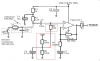
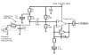
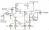
As you can see,i was confuse the function of R3 and why R5 and R6 act as voltage divider( I mean,it is compulsory to supply Vcc/2?).Part that i mark with red line was really confusing.Anyone can explain to me what happening there?:confused:

Thanks in advance!!
 

Attachments

  • Ts971 pre amp.JPG
    Ts971 pre amp.JPG
    46 KB · Views: 618
R3, along with C3 & C4 help filter out noise and hum from the Vcc power supply lead.
R4 prevents the audio signal from the mic from being bypassed to ground by C4.
You need R5 & R6 as a voltage divider to keep the TS461 in it's linear region. If the + terminal of the TS461 was not biased at all, then the output would sit at 0Vdc. Then when the AC signal from the mic was applied, only one half of the waveform would be reproduced because the output cannot go below ground potential (Negative supply rail).
 
Last edited:
R3, along with C3 & C4 help filter out noise and hum from the Vcc power supply lead.
R4 prevents the audio signal from the mic from being bypassed to ground by C4.
You need R5 & R6 as a voltage divider to keep the TS461 in it's linear region. If the + terminal of the TS461 was not biased at all, then the output would sit at 0Vdc. Then when the AC signal from the mic was applied, only one half of the waveform would be reproduced because the output cannot go below ground potential (Negative supply rail).

Thanks for your answer.Really appreciate it.:);)

How about C2 and C1?C2 is filtering noise from power supply and C1 bypass the audio signal from mic right?

Just want to justify my understanding.:eek:
 
I have made many mic preamps without R3 and C4.
C2 is needed with all electronic circuits that are battery-powered.

Many good opamps oscillate if they drive the capacitance of a shielded audio cable. Adding a 100 ohm resistor in series with the output of the circuit isolates the opamp from the capacitance of the cable so it does not oscillate.
 

Attachments

  • electret mic preamp.PNG
    electret mic preamp.PNG
    92.5 KB · Views: 1,726
I have made many mic preamps without R3 and C4.
C2 is needed with all electronic circuits that are battery-powered.

Many good opamps oscillate if they drive the capacitance of a shielded audio cable. Adding a 100 ohm resistor in series with the output of the circuit isolates the opamp from the capacitance of the cable so it does not oscillate.

Hai audio guru,

First of all,thank for your answer.Really appreciate it.:)

As kchriste said, the voltage divider is to keep the op amp in its linear region.Why it must Vcc/2?What it connection with rail to rail output?
 
The opamp is biased at Vcc/2 because it does not have a negative supply that is the same voltage as its positive supply. When the input is biased at Vcc/2 then its output idles at Vcc/2 so the output can swing positively the same amount as it can swing negatively for the max possible output level.
 
The opamp is biased at Vcc/2 because it does not have a negative supply that is the same voltage as its positive supply. When the input is biased at Vcc/2 then its output idles at Vcc/2 so the output can swing positively the same amount as it can swing negatively for the max possible output level.

Maybe i need to simulate it on lab and use oscilloscope to understand the concept.

I remove the R4,C3,R3 and C4 on the previous schematic.I think it should work same as previous schematic.
 

Attachments

  • Ts971 pre amp.JPG
    Ts971 pre amp.JPG
    36.3 KB · Views: 449
In the original post, R1/C1 make a filter that removes noise from the 2.7V supply from getting to the input of the amplifier. Also, R5,6/C3 makes a clean 1.35V supply.

In your last post, some of the noise on the 2.7 supply will go to the input of the amplifier. You could connect the top of R5 to C1.
 
How about C2 and C1?C2 is filtering noise from power supply and C1 bypass the audio signal from mic right?
In your original diagram, both C1 and C2 are there to filter noise from the power supply. While they also do filter any signal generated by the amplifier itself, their main function is power supply decoupling.
Most simulators will show no difference whether you include these caps or not. This is because the power supplies in simulators are perfect unless to degrade them with some noise from reality. ;)
 
Status
Not open for further replies.

Latest threads

New Articles From Microcontroller Tips

Back
Top