Continue to Site

Welcome to our site!

Electro Tech is an online community (with over 170,000 members) who enjoy talking about and building electronic circuits, projects and gadgets. To participate you need to register. Registration is free. Click here to register now.

  • Welcome to our site! Electro Tech is an online community (with over 170,000 members) who enjoy talking about and building electronic circuits, projects and gadgets. To participate you need to register. Registration is free. Click here to register now.

Doubt in circuit

Status
Not open for further replies.

dennis.roshan

New Member
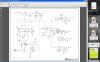
BQ 2002 IC and party analyzed circuit

BQ2002 IC decides wheather charging current flows from the DC source to the battery or not.

pin 4 is GND and pin 6 is Vcc. for the ic to work pin 6 is given to 6V and pin 4 to GND

Input pins
Vbat(pin 3) is monitored if this voltgae exceeds 2V then bq2002 stops the charging current. (i.e. max voltage in battery per cell. I have 4 cells)
Vtemp(pin 5) : the battery temp is measured via thermistor. this has a negative temp cofficient, so if temperature increases voltage decreases. if this voltage drops below 1.5v(excessive heating of battery has occurred) then bq2002 stops the charging current.
INH (pin7): this is an input pin, if this goes high then charging is stopped. if this is low then charging is continued. (bassically works like an intterupt).

if the charging is stopped by meeting any of the parameters then powers has to be restarted for the charging to continue.


Output pins
if BQ2002 decides to allow the charging current then the output pin8 CC goes to high impedance state(5.9V).
if BQ2002 decides to not allow the charging current then the output pin8 CC goes low (0V)
Ignore LED pin
TM decides the charging rate (C) in our case TM is connected to Vcc/2 to achieve C/4 charging current.
In the C/4 charge rate, if the charge time exceeds 320 min or 5hrs and 20 min bq2002 terminates the charging current.
in our case as seen in the schematic TM (pin1) is attached in between 24Kohm resistance between 6v and GND to get C/4 charge rate.

U14B is a comparator circuit. battery temp voltage is connected to pin 5(+ve terminal) if U14B, 2V is given to -ve terminal. this generates a low on pin 7 of U14B which is connected to INH pin. If a non rechargable is connected here then INH will go high, else it will be low.

D11,R73, R74, R75 is used to generate 5.5V which is given to pin 3 of U14A.

we know that CC (Pin 8) - if high impedance(5.9V) to allow charging current - if low stop charging current.

U14A is a comparator. it compares cc(Pin8) with 5.5V. if CC is high impedance then the output on pin 1 of U14A goes low which turns on the pnp power transistor which allows the charging current flow from the dc source to the battery. if CC is low then the output on pin 1 of U14A goes high which makes the pnp power transistor off which stops the charging current flow from the dc source to the battery.
U14A also works as an opamp as a current source. follow the link and compare with U14A circuit
http://www.eecs.tufts.edu/~dsculley/tutorial/opamps/opamps7.html
current = (+6V - Vref)/1ohm = .5A or 500 mA
Vref = 5.5V which is labeled as 0.5V(pin 3 of U14A) which means Vref is 0.5V below the +6V

this is the rought idea, the link below is the data sheet for BQ2002 it tells u what I summarized above
http://www.datasheetcatalog.org/datasheet/texasinstruments/bq2002t.pdf


I have connected a ammeter(multimeter in current mode) to measure to current in the circuit
Ammeter is connected between +6V & Vbat
according to the design 500mA current shd flow thru and the ammeter shd read 500mA
but this is not happening
I have drawn a red box for the circuit to be analysed. i have attached a JPG file for this.
I have also attached a PDF schematic.
 

Attachments

  • red_box.JPG
    red_box.JPG
    183 KB · Views: 374
  • Printing Print Schematic12.pdf
    63.9 KB · Views: 269
Ammeter is connected between +6V & Vbat
That will shunt out R59, Q3 and D9 and will be measuring (6-Vbat)/Rmeter. Try connecting it in series with R59, or between Q4 source and Vbat.
(And what is that rectangle attached to Q3 collector?)
(BTW, jpegs aren't good for schematics as small features are too fuzzy)
 
Last edited:
Hello Alec_t

I am sorry I was wrong. What I meant to say is,
The Rechargable NiMH battery I have has 3 terminals +ve terminal, -ve terminal and Vtemp
V_Batt is connedted to the +ve terminal of the battery,
-ve terminal of the battery is connected to the ground in the circuit
Vtemp is connected to Batt_temp in the circuit.

The ammeter is connected in series i.e. one terminal of the ammeter to the V_batt terminal and the other to the +ve of the battery.
 
Q3 is a power PNP transistor(2W), the item number is NJT4030PT, since it is designed to handle heavy current it has two collector terminals and this looks like a rectangle attatched.

The JPG file and the PDF file are the same, in the JPG file I have drawn a red box around the circuit to be analysed, this I could not do in the PDF file. I am sorry for the low res JPG, but the soul purpose of JPG is to indicate the part of the circuit to be analysed. For better schematics please refer PDF file.
 
Last edited:
the ammeter shd read 500mA but this is not happening
So what is happening? Current too high? Too low? Non-existent? Have you measured voltages at significant points (e.g. across R9, Q3 terminals)?
 
The current is an exponential decrease,
Sometimes it starts off with 70mA and decreases exponentially.
Sometimes it starts off with 50mA and decreases exponentially.

According to the design i should get constant 500mA of current during charge.
 
Last edited:
Hello Alec_t

During the charging operation; the +ve and -ve terminal of the battery behaves like a low resistor which can handle high current(500mA),
So I replaced the battery with 10ohm 6.5W resistor to simulate the battery. (I provided 1.6V on Batt_temp, this is mandatory to simulate the battery)
Now the current does not exponentially decrease but is constant at 120mA.
We can conclude there is some thing wrong with the battery, but there is also something wrong with the circuit since the current is not 500mA.
During this operation I do see that the source gives 400mA of current.
Any suggestions on how to analyse and debug this circuit?
 
I think the problem lies in the value of R64. The datasheet for Q3 quotes a hfe of min 200 at Ic = 1A. So for a collector current of 500mA the base current will be ~500/200 = 2.5mA (0.0025A). At 500mA R59 will drop 0.5V, so the voltage at Q3 base will be 6-0.5-0.6 = 4.9V. Assuming the op-amp U14A output can be driven as low as 0V (I haven't checked its spec) then R64 should be ~ 4.9/0.0025 = 1960 ohm to turn Q3 fully on. Allowing some margin, I'd suggest 1k maximum. So the present value of 15k is around eight times too high and will not enable Q3 to provide enough current. I'm surprised you get as much as 120mA; that suggests the hfe of your Q3 is above the minimum specified.
 
Hi Alec_t

I am sorry Q3 is not used in saturation. Q3(along with U14A) works as a constant current source hence it cannot be used in saturation. I am stilling trying to understand this part of the circuit.

I did the following analysis.

As mentioned earlier I simulated the battery by removing it connecting and I connected a power resistor (10ohm 6.5W) across the +ve and -ve terminal of the battery was connected. I also provided 1.6V dc voltage on Batt_temp terminal via external source.
The ammeter is connected in series i.e. one terminal of the ammeter to the V_batt terminal and the other to the power resistor, this is to measure the load/charge current.

The external power supply is set at 6V
When both the Diodes D10 and D14 are connected, the 6V power supply showed that I am drawing 0.4A and the charge current reading was 120mA.
When the Diode D10 is connected and D14 is removed, the 6V power supply showed that I am drawing 0.3A and the charge current reading was 120mA.
When both the Diodes D10 and D14 are removed, the 6V power supply showed that I am drawing 0.13A and the charge current reading was 120mA.

On the right side of D14 there exists a circuit that draws roughly 100mA of current which is reasonable. But D10 (or the circuit on the right side of D10) is consuming 170mA of current which is weird. D10 is a Zener diode with a knee voltage of 10V I found out that this is broken because at 6V under reverse bias it was conducting when it is supposed to conduct at 10V. Anyways D10 is for reverse current protection, its presence will not affect the circuit that I want to analyse (i.e. the circuit in red box.), so I removed D10.
Also if I cut the path between D10 and C71, the 6V power supply shows 0.0A drawn from the source and the charge current is zero. If it is shorted back then the current flows in the circuit(red box circuit) that I want to analyse.

Now I did remove both the diodes. The external power supply is set at 6V and it shows I am drawing 0.13A of current and the charge current is 112-120mA. The ammeter reading is supposed to be 500mA, but it is 112-120mA. To test the constant current source I did vary the power resistor(i.e. the battery power resistor).
I have one 10ohm 6.5W resistor and I also have two 7.5ohm 5W resistor
I connected 10ohm 6.5W I got charge current to be 120mA
I connected 7.5ohm 5W I got chrage current to be 123/124mA
I made 7.5ohm 5W parallel 7.5ohm 5W (net resistance = 3.75Ohm) this gave me 128mA
Finally I made 10ohm series with 7.5ohm (net resistance of 17.5ohm) this gave me charge current to be 97mA.

The constant current source is not so good (the varition of power resistor inturn varies the load/charge current). I am still trying to understand Q3, U14A and how the values of R60, R64, R68, R70 and C70 were assigned to it?

I some how think R64 (base resistance) needs to be calibrated.
Can you please help me in this circuit?
Thank you.
 
Last edited:
Ok, so the DPLS350E has a similar hfe spec and my analysis holds, except that when I said "R64 should be ~ 4.9/0.0025 = 1960 ohm to turn Q3 fully on" I should have said "R64 should be ~ 4.9/0.0025 = 1960 ohm to give a 500mA current through Q3". Apologies. I appreciate that Q3 isn't being (indeed shouldn't be) used in saturation. By the way, if that transistor is rated at 1W it will be severely stressed trying to charge a nearly-flat battery at 0.5A. If Vbat were 3V then there would be 2.5V across Q3. 2.5V * 0.5A = 1.25W! I'd replace it with a beefier transistor.
I'd try R64 = 1k and see if that improves things. Not sure what you mean by it 'needs to be calibrated'.
It's a puzzle why disconnecting the link between D10 and C71 should reduce the charge current to zero. Clearly it will prevent U17 from generating 12V. Are you sure some of the terminals labelled '+6.0V' aren't being fed indirectly from that 12V supply? What supplies U14Pwr?
I think your experiments with varying the load resistor show that the 'constant current' feature is working (after a fashion!).
 
Last edited:
I've spotted an error in the circuit. By virtue of R73, R74, D11 the reference voltage at U14A pin 3 will be 5.5V, not 0.5V as shown. Without knowing the voltage at pin 8 of U15 it is difficult to tell whether the correct U14A reference should be 0.5V or 5.5V.
Another puzzle. R62, R63 are a voltage divider with a 4:1 division ratio. Their junction point is marked '2V max', suggesting Vbat could be up to 8V. You're never going to charge an 8V battery with a 6V supply!
 
Last edited:
On further analysis of the circuit I've sussed how the constant current control is supposed to work. The correct reference voltage at U14A pin3 is 5.5V (so there's a typo on the schematic, the values of R73 and R74 are ok). However, if R75 is 20k as shown then the current through zener D11 is (6-4.7)/20k = 65uA. IMHO that's far too small to give a reliable knee voltage and may well account for why you experienced drift in the measured dummy load current. A value of <=1k would give a zener current of >=1.3mA and a more 'solid' reference.
Op-amp U14A will try to maintain the voltage at pin 2 at 5.5V, hence the voltage drop across R59 will be kept at 6-5.5=0.5V (ignoring for now the effect of the current-control voltage from the CC pin 8 of U15) and the current through R59 and the battery will thus be 500mA.
Now consider the effect of the voltage at CC (let's just call it V, and call the voltage at Q3 emitter E).
(1) Assume V=6. So R70 drops 6-5.5=0.5V. But R68 is half R70, so R68 drops 0.25V. So E = 5.5-0.25 = 5.25. Thus the R59 current will be 6-5.25 = 0.75A. That is the maximum charge/short-circuit current the charger will provide.
(2) Assume V=0. U14A will try to adjust Q3 current and E so that pin 2 is at 5.5V but it can't. U14A output goes to ~6V and Q3 cuts off (load current = 0), with E at 6V and pin 2 at 6*20k/(20k+10k) = 4V.

Under short-circuit load conditions Q3 will dissipate 6V*0.75A = 4W. The specified transistor is not adequately rated for that.
 
The CC is the open-drain output.
So your first assumption (Assume V=6) is wrong.
And probably R75 is equal to 2k.
And you're doing pretty good job with the analysis of tis circuit.
 
Last edited:
Thanks for that, Jony130. I'm not familiar with the U15 chip but was just taking two extreme values (0, 6) to see the effects of varying the CC voltage. I stand corrected.
So if CC is open-drain E won't go below 5.5V, the maximum R59 current is 500mA, and Q3 power dissipation with a short-circuited load is 3W.
I agree that R75 was probably meant to be 2k rather than 20K, but even that seems too high.
I've now found where U14Pwr is derived (at U14B).
Yet another oddity: Q8 drain voltage can apparently be up to 6.3 V according to the schematic. How, with a 6V supply????
 
Status
Not open for further replies.

New Articles From Microcontroller Tips

Back
Top