HankMcSpank
New Member
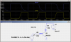
Well it's looking like the most viable solution (low parts count, lowish current) is to simply go with my first schematic (two fets), but bring the value of the 1st fet drain resistor down to about 3.3k...but also add in one extra resistor above it (so now, the first fet drain will have both a 3.3k and 660R resistor connecting to 9V) ...and then take the 'junction' of the two resistors to the p mosfet gate - job done.
The litmus test wrt how successful the revised switching waveform is....is simply to look at the LEDs (ie the load). With a 16khz switching waveform at a duty cycle of 1/256th, the LEDs should be barely visibly on ...beforehand, at 1/256th duty cycle they were too visibly on (this being due to the aforementioned CR induced slope essentially extending the duty cycle on/off ratio to the LEDs) ...but by reducing the drain resistor value (therefore less CR induced slope) and adding in an extra resistor to form a potential divider on the switching waveform (therefore the P-chan gate now only sees 9V-> 8V(ish) switching voltage vs 9V->0V with just one drain resistor), the LEDs are indeed now very low intensity at a duty cycle of 1/256th (being high brightness leds, even a duty cycle of 1/256th has them discernibly 'on'.) When the N channel is on, there's about 3mA flowing through the two resistors (attributed to the switching on/off the p chan mosfet)...I'd have preferred less, but I can live with it.
Thanks for all your input.
Last edited: