Hi,
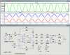
I´m having some problems understand a circuit. We are using a a differntial ADC driver, the ADA4937 before the input to the ADC (AD9640).
Please find attached our circuit and the data sheet of the differential driver. We would be very grateful if someone could shed some light on the following questions:
1) We have a differntial signal applied to the inputs of the differential driver. If these inputs go negative, what will happen given that the ADA4937 does not have a -ve supply? Must the applied differential signal have a DC bias ideally in the mid point of the power supply? (The power supply is 3.3V)
2)It does not seem to be specified in the datasheet what the maximum voltage levels can be on the inputs to the differential driver. I was expecting it to say something like the limit would be the from gnd to Vcc but I cannot find any reference to it.
3) Can someone explain what a differential analog signal would look like in relation to a single ended signal?
Many thanks for any help
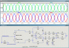
")