Continue to Site

Welcome to our site!

Electro Tech is an online community (with over 170,000 members) who enjoy talking about and building electronic circuits, projects and gadgets. To participate you need to register. Registration is free. Click here to register now.

  • Welcome to our site! Electro Tech is an online community (with over 170,000 members) who enjoy talking about and building electronic circuits, projects and gadgets. To participate you need to register. Registration is free. Click here to register now.

designing system with Flip Flops

Status
Not open for further replies.

electroRF

Member
Hi,

I'm trying to write a block diagram of the following system:

The system gets control bit = r/w'
and it gets m-bit address

when r/w' = 1 (read), it reads the content of that memory address from a memory, and output it on n-data bus.

when r/w' = 0 (write), it reads the content of that memory address from a memory, increment the content by 1, and write it back into the memory address.

The memory itself is given as a black box - no need to design it.


How would you design the rest using Flip-Flops / Mux / Counter / etc (synchronized discrete components)

I sketched it, but I don't know how to translate it into Flip-Flops:

Thank you!
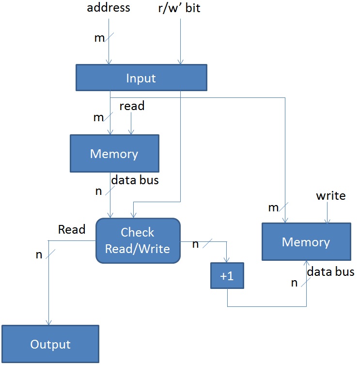
memorydesign.jpg
 
I don't understand your flow chart too well. Can you explain what you are trying to accomplish ... at least to some extent?
 
Hi User,
Thank you for helping.

1. The system gets m-bit address and 1-bit r/w' control signal

2. The system then reads the memory's content

3. if r/w' bit = 1 (READ), the content is transferred to the output of the system

4. else, if r/w' bit = 0 (WRITE), the content is incremented by 1, and is written into the memory.

Does that explain it better?
 
This is a part of an ALU that executes the command INC "increment" form a set of registers (user memories)
Here we need to remember something, the register normally have input buss and output buss while the memory have common buss.
with a common buss you can NOT put the result over the original data, that will destroy the hardware, even if you use registers with separate busses, you get what is called rabbet race which is the output is incremented and fed back to the same part then it will be an output immediately to be incremented again and again.
That is why there must be a system clock that times when each action must happen and a sequencer that enables each part to do its job at its correct time
 
There is a book... "The art of electronics" They teach you to build a small computer...

I suggest trying to get hold of a copy..... All that's needed is shift registers with parallel and serial load..
 
shift registers won't increment, so you'll also need some kind of counter; but you can use a serial to parallel shift register (plus xor gates) to create a sequencer. Also, there is no "Address Latch Enable" to tell when you have a valid address/r/w command (or enable, or start command input).

So, here are the commands you'll need to generate:
Read: 1) disable output oe 2) enable memory output enable (oe) 3) latch data to output register 4) disable memory oe, enable output oe 5) issue end cmd (reset start f/f)
Write: 1) disable output oe (last command could've been read) 2) enable mem oe, enable buffer 1 oe (memory to counter register) 3) latch data into ctr register 4) disable mem oe, buff1 oe, inc ctr 5) enable buffer 2 oe (ctr to memory) 6) enable memory write 7) disable memory write 8) disable buffer 2 oe 9) issue end cmd (reset start f/f)

The above command sequence assumes:
1) the memory is cs enabled all the time (chip select).
2) you only output on a read command.
3) separate ctr/output buffers. These can, of course, be combined into one.
4) Uses output buffer register so output doesn't change as memory address changes, until start command.
 
Here is the block diagram to go with the sequencer commands listed above...
 

Attachments

  • block.pdf
    37 KB · Views: 209
Mike,
I can't thank you enough!

I'm studying your design at the moment! :)

I have 2 questions please:

1. there's the READ sequencer and the WRITE sequencer.

When the r/w' bit is 1, the READ seq. receives 1 into its inverted input and the WRITE seq. receives 0 into its inverted input.

What is the duty (purpose) of the inverted input? does it act as enable / disable?

2. what is the purpose of the POR signal?


Thank you very much.
 
The sequencers use a 74HC164 serial to parallel shift register. Basically, the system clock sends a '1' through it. The inverted inputs I'm using are the Master Clear pins, that reset the device when held low, so all outputs are '0', and when it goes hi it allows the one to be shifted through. When you bring it back low, it resets all outputs (and internal registers) to '0'.

The POR is Power On Reset, basically an RC tied to an inverter chip. This is just a block diagram, and doesn't show actual chip hookups. However, each block is a group of logic chips.
 
Status
Not open for further replies.

Latest threads

Back
Top