Continue to Site

Welcome to our site!

Electro Tech is an online community (with over 170,000 members) who enjoy talking about and building electronic circuits, projects and gadgets. To participate you need to register. Registration is free. Click here to register now.

  • Welcome to our site! Electro Tech is an online community (with over 170,000 members) who enjoy talking about and building electronic circuits, projects and gadgets. To participate you need to register. Registration is free. Click here to register now.

designing MOSFET inverter

Status
Not open for further replies.

PG1995

Active Member
Hi

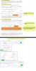
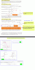
Could you please help me with these queries? These relate to noise margins of NMOS inverter. Thank you.

Regards
PG
 

Attachments

  • mosfet_noise_margin.jpg
    mosfet_noise_margin.jpg
    672 KB · Views: 295
Hi,


Since nobody answered yet i'll start by helping with Q1. See attachment.

Since they solved for V_IL (6.17 left), we have one thing solved for already. So take that and substitute that into equation 6.15 for v_I and that
gives us V_OH because V_IL corresponds to V_OH on the input/output curve.

So in other words once you have the input voltage that corresponds to some output voltage you can go back and substitute into the equation for 'vo' to get the corresponding output voltage.

BTW, the exact value for that constant "1.63" is really:
2*sqrt(2)/sqrt(3)

You'll need that to get the same exact result they got for 6.19 right (Q2).
 

Attachments

  • Mosfet_Noise_Margin.gif
    Mosfet_Noise_Margin.gif
    286.2 KB · Views: 260
Last edited:
Thank you, MrAl.

I have included my own little understandING of the noise margin which might be helpful to someone like me.

Regards
PG
 

Attachments

  • electronics_noise_margin2.jpg
    electronics_noise_margin2.jpg
    228.2 KB · Views: 278
Last edited:
Hello again,

I'll have to read that over to see what you mean.

Basically if you design a Schmitt Trigger you note that you have to have high enough gain to get the output to SHOOT up (or down) to the next logic level. With the gain too low, the dang output follows the input signal. The problem is that at some point the gain is too low in the transition region and that means the output follows the input for a time and that is considered a no no for logic because the output is supposed to be well defined even if the input isnt. This is one of the reasons why we look for unity slope to help define noise margin. Contrast this with noise immunity for more enlightenment.

We could look at a couple designs to see how this happens but i have a feeling you dont want to take the time right now.
 
Thank you, MrAl.

We could look at a couple designs to see how this happens but i have a feeling you dont want to take the time right now.

Yes, that's right but I would say I don't have the time, and further the capacity to understand this stuff in detail at such basic level. But I'm sure someday we can discuss those designs in detail. Thank you.

Best regards
PG
 
Hi

Could someone please help me with the query in the last post? Thanks.

Regards
PG


PS: I have found the answer.


For example, n+ denotes an n-type semiconductor with a high, often degenerate, doping concentration. Similarly, p- would indicate a very lightly doped p-type material.

When many more dopant atoms are added, on the order of one per ten thousand atoms, the doping is referred to as heavy or high. This is often shown as n+ for n-type doping or p+ for p-type doping.


References:
1: https://en.wikipedia.org/wiki/Doping_(semiconductor)
2: https://en.wikipedia.org/wiki/Extrinsic_semiconductor
3: https://en.wikipedia.org/wiki/Degenerate_semiconductor
 
Last edited:
Hi,

I didnt even notice that post was there until you posted again. Must have missed it somehow. Happy you found the answer.
 
Status
Not open for further replies.

Latest threads

New Articles From Microcontroller Tips

Back
Top